MB95630H Series
MN702-00009-1v0-E
FUJITSU SEMICONDUCTOR LIMITED
555
CHAPTER 25 DUAL OPERATION FLASH MEMORY
25.6 Operations
25.6
Operations
Pay attention in particular to the following points when using dual operation
Flash memory:
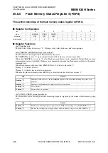
• Interrupt generated when upper banks are updated
• Procedure of setting the sector swap enable bit in the flash memory status
register (FSR:SSEN)
■
Interrupt Generated When Upper Banks Are Updated
The dual operation Flash memory consists of two banks. Like conventional Flash products,
however, it cannot be erased/programmed and read at the same time in banks on the same side.
As SA2 contains an interrupt vector, an interrupt vector from the CPU cannot be read normally
when an interrupt occurs during programming data to an upper bank. Before an upper bank can
be updated, the sector swap enable bit must be set to "1" (FSR:SSEN = 1). When an interrupt
occurs, therefore, SA1 is accessed to read interrupt vector data. The same data must be copied
to SA1 and SA2 before the sector swap enable bit (FSR:SSEN) is set.
■
Procedure for Setting Sector Swap Enable Bit (FSR:SSEN)
Figure 25.6-1 shows a sample procedure of setting the sector swap enable bit (FSR:SSEN).
To modify data in the upper bank, it is necessary to set FSR:SSEN to "1". While data is being
written to the Flash memory, modifying the setting of FSR:SSEN is prohibited. The setting of
FSR:SSEN can only be modified before the start of programming data to the Flash memory or
after the completion of programming data to the Flash memory. In addition, control the Flash
memory interrupts while setting FSR:SSEN as follows: before setting FSR:SSEN, disable the
Flash memory interrupts; after setting FSR:SSEN, enable the interrupts.
Figure 25.6-1 Sample Procedure for Setting the Sector Swap Enable Bit (FSR:SSEN)
S
t
a
rt
u
pd
a
ting Fl
as
h d
a
t
a
S
t
a
rt progr
a
m oper
a
tion
Copy d
a
t
a
from
S
A2 to
S
A1
S
t
a
rt progr
a
m oper
a
tion
Complete
Fl
as
h d
a
t
a
u
pd
a
te
Complete
Fl
as
h d
a
t
a
u
pd
a
te
S
et F
S
R:
SS
EN to "1"
S
et F
S
R:
SS
EN to "0"
Upd
a
te d
a
t
a
in
u
pper
ba
nk
Upd
a
te d
a
t
a
in lower
ba
nk
Содержание MB95630H Series
Страница 2: ......
Страница 4: ......
Страница 8: ...iv ...
Страница 20: ...xvi ...
Страница 106: ...MB95630H Series 86 FUJITSU SEMICONDUCTOR LIMITED MN702 00009 1v0 E CHAPTER 6 I O PORT 6 2 Configuration and Operations ...
Страница 282: ...MB95630H Series 262 FUJITSU SEMICONDUCTOR LIMITED MN702 00009 1v0 E CHAPTER 14 LIN UART 14 8 Notes on Using LIN UART ...
Страница 642: ...MB95630H Series 622 FUJITSU SEMICONDUCTOR LIMITED MN702 00009 1v0 E APPENDIX A Instruction Overview A 5 Instruction Map ...
Страница 644: ......


