MB95630H Series
450
FUJITSU SEMICONDUCTOR LIMITED
MN702-00009-1v0-E
CHAPTER 21 MULTI-PULSE GENERATOR
21.7 Notes on Using Multi-pulse Generator
21.7
Notes on Using Multi-pulse Generator
This section provides notes on using the multi-pulse generator.
■
Notes on Using Waveform Sequencer
●
Notes on using a program for setting
•
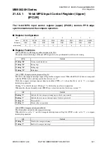
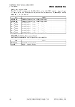
Directly changing from one PPG synchronization mode to another PPG synchronization
mode (e.g. from rising-edge synchronization (IPCUR:WTS[1:0] = 0b01) to falling-edge
synchronization (IPCUR:WTS[1:0] = 0b10) or vice versa) is prohibited. To change from
one PPG synchronization mode to another PPG synchronization mode, disable PPG edge
synchronization (IPCUR:WTS[1:0] = 0b00) temporarily before changing to another PPG
synchronization mode.
•
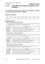
When the data transfer method is changed, the next data buffer register to be selected is
always specified by the BNKF bit and RDA[2:0] bits in the 16-bit MPG output data register
(upper) (OPDUR). However, this does not apply to the OPDBRH0/OPDBRL0 write
method (OPCUR:OPS[2:0] = 0b000). In the OPDBRH0/OPDBRL0 write method, the
BNKF bit and RDA[2:0] bits are ignored.
•
To access the 16-bit MPG output data register (upper/lower) (OPDUR/OPDLR), the word
access instruction must be used. Use the "MOVW" instruction to access OPDUR and
OPDLR, or use the "MOV" instruction to access OPDUR first and then OPDLR.
•
When using the OPDBRH0/OPDBRL0 write method for data transfer (OPCUR:OPS[2:0] =
0b000), word access to output data buffer register 0 must be used, byte access to either
lower register or upper register does not start any transfer operation.
•
In order to use the 16-bit reload timer underflow transfer method
(OPCUR:OPS[2:0] = 0b010), the reload timer should be used in reload mode. Software
trigger is needed to be used for the startup of the reload timer. The 16-bit reload timer is
needed for setting the update time in advance and executing the continuous control action.
•
In order to use the position detection and timer underflow transfer method
(OPCUR:OPS[2:0] = 0b011 or 0b111), the reload timer should be used in one-shot mode.
TIN0O must be longer than two machine cycles.
•
Before the DTTI circuit is enabled (OPCUR:DTIE = 1), make sure that the port x which is
multiplexed with the OPTx is configured as an output port by setting its port direction
register (DDRx).
•
Since the DTTI input control circuit uses a peripheral clock, input is invalidated even if the
DTTI input is enabled (OPCUR:DTIE = 1) in a mode such as stop mode in which the
oscillator stops.
•
In the worst situation, the time from DTTI being recognized (after noise cancellation) to
DTISP in effect takes two cycles; in the best situation, it takes one cycle.
•
Before modifying the D[1:0] bits in the 16-bit MPG noise cancellation control register
(NCCR), ensure that the noise cancellation function has been disabled (OPCUR:NRSL = 0).
•
Before modifying the S2[1:0], S1[1:0] and S0[1:0] bits in the NCCR register, ensure that
the noise cancellation function has been disabled (IPCLR:SNC[2:0] = 0b000).
Содержание MB95630H Series
Страница 2: ......
Страница 4: ......
Страница 8: ...iv ...
Страница 20: ...xvi ...
Страница 106: ...MB95630H Series 86 FUJITSU SEMICONDUCTOR LIMITED MN702 00009 1v0 E CHAPTER 6 I O PORT 6 2 Configuration and Operations ...
Страница 282: ...MB95630H Series 262 FUJITSU SEMICONDUCTOR LIMITED MN702 00009 1v0 E CHAPTER 14 LIN UART 14 8 Notes on Using LIN UART ...
Страница 642: ...MB95630H Series 622 FUJITSU SEMICONDUCTOR LIMITED MN702 00009 1v0 E APPENDIX A Instruction Overview A 5 Instruction Map ...
Страница 644: ......


