


MPC563XM Reference Manual, Rev. 1
280
Freescale Semiconductor
Preliminary—Subject to Change Without Notice
have different access time characteristics. These wait-states are applied in addition to the normal
wait-states incurred for Flash accesses. Refer to
Section 11.7.11, “Wait-State Emulation
” for more details.
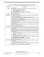
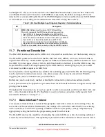
11.7.2
Access Protections
The Flash BIU provides programmable configurable access protections for both read and write cycles from
masters via the CFLASH_BIU2 register. It allows restriction of read and write requests on a per-master
basis. This functionality is described in the dedicated section. Detection of a protection violation results in
an error response from the Flash BIU on the AHB transfer.
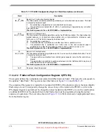
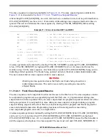
11.7.3
Read Cycles - Buffer Miss
Read cycles from the Flash array are initiated by driving a valid access address . The Flash BIU then waits
for the programmed number of read wait states before sampling the read data . This data is normally stored
in the least-recently updated page read buffer for bank0 in parallel with the requested data being forwarded
to the AHB.
If the Flash access was the direct result of an AHB transaction, the page buffer is marked as
most-recently-used as it is being loaded. If the Flash access was the result of a speculative prefetch to the
next sequential line, it is first loaded into the least-recently-used buffer. The status of this buffer is not
changed to most-recently-used until a subsequent buffer hit occurs.
11.7.4
Read Cycles - Buffer Hit
Single cycle read responses to the AHB are possible with the Flash BIU when the requested read access
was previously loaded into one of the bank0 page buffers. In these “buffer hit” cases, read data is returned
to the AHB data phase with a zero wait-state response.
Likewise, the bank1 logic includes a single 128-bit temporary holding register and sequential accesses
which “hit” in this register are also serviced with a zero wait-state response.
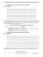
11.7.5
Write Cycles
In a write cycle, address, write data, and control signals are launched at the completion of the first AHB
data phase cycle. Write cycles to the Flash array are initiated by driving a valid access address
11.7.6
Error Termination
The Flash BIU follows the standard procedure when an AHB bus cycle is terminated with an ERROR
response. The first case that can cause an error response to the AHB is when an access is attempted by an
AHB master whose corresponding Read Access Control or Write Access Control settings do not allow the
access, thus causing a protection violation. In this case, the Flash BIU does not initiate a Flash array access.
The second case that can cause an error response to the AHB is when an access is performed to the Flash
array and is terminated with a Flash error response. This may occur for either a read or a write operation.
Содержание MPC5632M
Страница 22: ...MPC563XM Reference Manual Rev 1 22 Freescale Semiconductor Preliminary Subject to Change Without Notice ...
Страница 62: ...MPC563XM Reference Manual Rev 1 62 Freescale Semiconductor Preliminary Subject to Change Without Notice ...
Страница 92: ...MPC563XM Reference Manual Rev 1 92 Freescale Semiconductor Preliminary Subject to Change Without Notice ...
Страница 168: ...MPC563XM Reference Manual Rev 1 168 Freescale Semiconductor Preliminary Subject to Change Without Notice ...
Страница 242: ...MPC563XM Reference Manual Rev 1 242 Freescale Semiconductor Preliminary Subject to Change Without Notice ...
Страница 302: ...MPC563XM Reference Manual Rev 1 302 Freescale Semiconductor Preliminary Subject to Change Without Notice ...
Страница 410: ...MPC563XM Reference Manual Rev 1 410 Freescale Semiconductor Preliminary Subject to Change Without Notice ...
Страница 440: ...MPC563XM Reference Manual Rev 1 440 Freescale Semiconductor Preliminary Subject to Change Without Notice ...
Страница 464: ...MPC563XM Reference Manual Rev 1 464 Freescale Semiconductor Preliminary Subject to Change Without Notice ...
Страница 554: ...MPC563XM Reference Manual Rev 1 554 Freescale Semiconductor Preliminary Subject to Change Without Notice ...
Страница 590: ...MPC563XM Reference Manual Rev 1 590 Freescale Semiconductor Preliminary Subject to Change Without Notice ...
Страница 622: ...MPC563XM Reference Manual Rev 1 622 Freescale Semiconductor Preliminary Subject to Change Without Notice ...
Страница 716: ...MPC563XM Reference Manual Rev 1 716 Freescale Semiconductor Preliminary Subject to Change Without Notice ...
Страница 1114: ...MPC563XM Reference Manual Rev 1 1114 Freescale Semiconductor Preliminary Subject to Change Without Notice ...
Страница 1144: ...MPC563XM Reference Manual Rev 1 1144 Freescale Semiconductor Preliminary Subject to Change Without Notice ...
Страница 1266: ...MPC563XM Reference Manual Rev 1 1266 Freescale Semiconductor Preliminary Subject to Change Without Notice ...
Страница 1316: ...MPC563XM Reference Manual Rev 1 1316 Freescale Semiconductor Preliminary Subject to Change Without Notice ...
Страница 1348: ...MPC563XM Reference Manual Rev 1 1348 Freescale Semiconductor Preliminary Subject to Change Without Notice ...
Страница 1362: ...MPC563XM Reference Manual Rev 1 1362 Freescale Semiconductor Preliminary Subject to Change Without Notice ...
Страница 1382: ...MPC563XM Reference Manual Rev 1 1382 Freescale Semiconductor Preliminary Subject to Change Without Notice ...


