


MPC563XM Reference Manual, Rev. 1
Freescale Semiconductor
279
Preliminary—Subject to Change Without Notice
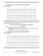
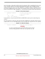
including ECC): bits 23-16 are ECC bits for the odd Double Word and bits 7-0 are the ECC bits for the
even Double Word; bits 27-26 and 11-10 of MISR are respectively the double and single ECC error
detection for even and odd Double Word. The UMISR4 Register is not accessible whenever MCR.DONE
or UT0.AID are low: reading returns indeterminate data while writing has no effect.
11.7
Functional Description
The Flash BIU interfaces between the AHB-Lite 2.v6 system bus and the low-cost Flash memory array(s).
The Flash BIU generates read and write enables, the Flash array address, write size, and write data as
inputs to the Flash array. The Flash BIU captures read data from the Flash array interface and drives it onto
the AHB. Up to four pages of data (128-bit width) from bank0 are buffered by the Flash BIU. Lines may
be prefetched in advance of being requested by the AHB interface, allowing single-cycle (zero AHB
wait-states) read data responses on buffer hits.
Several prefetch control algorithms are available for controlling page read buffer fills. Prefetch triggering
may be restricted to instruction accesses only, data accesses only, or may be unrestricted. Prefetch
triggering may also be controlled on a per-master basis.
Buffers may also be selectively enabled or disabled for allocation by instruction and data prefetch.
Access protections may be applied on a per-master basis for both reads and writes to support security and
privilege mechanisms.
Throughout this discussion,
bkn_
is used as a prefix to refer to two signals, each for each bank:
bk0_
and
bk1_
. Also, the nomenclature Bx_Py_RegName is used to reference a program-visible register field
associated with bank “x” and port “y”.
11.7.1
Basic Interface Protocol
Accesses are terminated under control of the appropriate read/write wait state control setting. Thus, the
access time of the operation is determined by the settings of the wait-state control fields. Access timing
can be varied to account for the operating conditions of the SoC (frequency, voltage, temperature) by
appropriately setting the fields in the programming model for either bank.
The Flash BIU also has the capability of extending the normal AHB access time by inserting additional
wait states for reads and writes. This capability is provided to allow emulation of other memories which
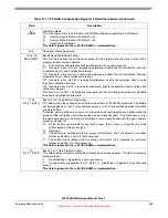
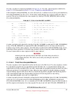
Table 11-26. User Multiple Input Signature Register 4 field descriptions
Bit
Description
0-31
MS159-128
:
Multiple input Signature 159-128
(Read/Write)
These bits represents the MISR value obtained accumulating:
• the 8 ECC bits for the even Double Word (on MS135-128)
• the single ECC error detection for even Double Word (on MS138)
• the double ECC error detection for even Double Word (on MS139)
• the 8 ECC bits for the odd Double Word (on MS151-144)
• the single ECC error detection for odd Double Word (on MS154)
• the double ECC error detection for odd Double Word (on MS155).
The MS can be seeded to any value by writing the UMISR4 register.
Содержание MPC5632M
Страница 22: ...MPC563XM Reference Manual Rev 1 22 Freescale Semiconductor Preliminary Subject to Change Without Notice ...
Страница 62: ...MPC563XM Reference Manual Rev 1 62 Freescale Semiconductor Preliminary Subject to Change Without Notice ...
Страница 92: ...MPC563XM Reference Manual Rev 1 92 Freescale Semiconductor Preliminary Subject to Change Without Notice ...
Страница 168: ...MPC563XM Reference Manual Rev 1 168 Freescale Semiconductor Preliminary Subject to Change Without Notice ...
Страница 242: ...MPC563XM Reference Manual Rev 1 242 Freescale Semiconductor Preliminary Subject to Change Without Notice ...
Страница 302: ...MPC563XM Reference Manual Rev 1 302 Freescale Semiconductor Preliminary Subject to Change Without Notice ...
Страница 410: ...MPC563XM Reference Manual Rev 1 410 Freescale Semiconductor Preliminary Subject to Change Without Notice ...
Страница 440: ...MPC563XM Reference Manual Rev 1 440 Freescale Semiconductor Preliminary Subject to Change Without Notice ...
Страница 464: ...MPC563XM Reference Manual Rev 1 464 Freescale Semiconductor Preliminary Subject to Change Without Notice ...
Страница 554: ...MPC563XM Reference Manual Rev 1 554 Freescale Semiconductor Preliminary Subject to Change Without Notice ...
Страница 590: ...MPC563XM Reference Manual Rev 1 590 Freescale Semiconductor Preliminary Subject to Change Without Notice ...
Страница 622: ...MPC563XM Reference Manual Rev 1 622 Freescale Semiconductor Preliminary Subject to Change Without Notice ...
Страница 716: ...MPC563XM Reference Manual Rev 1 716 Freescale Semiconductor Preliminary Subject to Change Without Notice ...
Страница 1114: ...MPC563XM Reference Manual Rev 1 1114 Freescale Semiconductor Preliminary Subject to Change Without Notice ...
Страница 1144: ...MPC563XM Reference Manual Rev 1 1144 Freescale Semiconductor Preliminary Subject to Change Without Notice ...
Страница 1266: ...MPC563XM Reference Manual Rev 1 1266 Freescale Semiconductor Preliminary Subject to Change Without Notice ...
Страница 1316: ...MPC563XM Reference Manual Rev 1 1316 Freescale Semiconductor Preliminary Subject to Change Without Notice ...
Страница 1348: ...MPC563XM Reference Manual Rev 1 1348 Freescale Semiconductor Preliminary Subject to Change Without Notice ...
Страница 1362: ...MPC563XM Reference Manual Rev 1 1362 Freescale Semiconductor Preliminary Subject to Change Without Notice ...
Страница 1382: ...MPC563XM Reference Manual Rev 1 1382 Freescale Semiconductor Preliminary Subject to Change Without Notice ...


