


MPC563XM Reference Manual, Rev. 1
1360
Freescale Semiconductor
Preliminary—Subject to Change Without Notice
31.5.4.6
CLAMP Instruction
CLAMP allows the state of signals driven from MCU pins to be determined from the boundary scan
register while the bypass register is selected as the serial path between TDI and TDO. CLAMP enhances
test efficiency by reducing the overall shift path to a single bit (the bypass register) while conducting an
EXTEST type of instruction through the boundary scan register. CLAMP also asserts the internal system
reset for the MCU to force a predictable internal state.
31.5.4.7
ACCESS_AUX_TAP_x Instructions
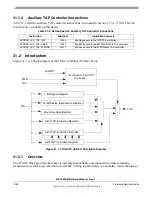
The JTAGC is configurable to allow up to fifteen other TAP controllers on the device to share the port with
it. This is done by providing ACCESS_AUX_TAP_x instructions for each of these TAP controllers. When
this instruction is loaded, control of the JTAG pins are transferred to the selected TAP controller. Any data
input via TDI and TMS is passed to the selected TAP controller, and any TDO output from the selected
TAP controller is sent back to the JTAGC to be output on the pins. The JTAGC regains control of the JTAG
port during the UPDATE-DR state if the PAUSE-DR state was entered. Auxiliary TAP controllers are held
in RUN-TEST/IDLE while they are inactive. Instructions not used to access an auxiliary TAP controller
on a device are treated like the BYPASS instruction.
31.5.4.8
BYPASS Instruction
BYPASS selects the bypass register, creating a single-bit shift register path between TDI and TDO.
BYPASS enhances test efficiency by reducing the overall shift path when no test operation of the MCU is
required. This allows more rapid movement of test data to and from other components on a board that are
required to perform test functions. While the BYPASS instruction is active the system logic operates
normally.
31.5.5
Boundary Scan
The boundary scan technique allows signals at component boundaries to be controlled and observed
through the shift-register stage associated with each pad. Each stage is part of a larger boundary scan
register cell, and cells for each pad are interconnected serially to form a shift-register chain around the
border of the design. The boundary scan register consists of this shift-register chain, and is connected
between TDI and TDO when the EXTEST, SAMPLE, or SAMPLE/PRELOAD instructions are loaded.
The shift-register chain contains a serial input and serial output, as well as clock and control signals.
The JTAGC supports the use of two possible boundary scan techniques. The first technique uses an internal
boundary scan register coupled with external pad/padi control to implement the BC cells. The second
technique fully implements the boundary scan register and BC cells outside of the module. When using
the second boundary scan technique, the function of the JTAGC is to provide the TDO output of the
external boundary scan register to the TDO pin, while not using the internal boundary scan register at all.
31.6
Initialization/Application Information
The test logic is a static logic design, and TCK can be stopped in either a high or low state without loss of
data. However, the system clock is not synchronized to TCK internally. Any mixed operation using both
the test logic and the system functional logic requires external synchronization.
Содержание MPC5632M
Страница 22: ...MPC563XM Reference Manual Rev 1 22 Freescale Semiconductor Preliminary Subject to Change Without Notice ...
Страница 62: ...MPC563XM Reference Manual Rev 1 62 Freescale Semiconductor Preliminary Subject to Change Without Notice ...
Страница 92: ...MPC563XM Reference Manual Rev 1 92 Freescale Semiconductor Preliminary Subject to Change Without Notice ...
Страница 168: ...MPC563XM Reference Manual Rev 1 168 Freescale Semiconductor Preliminary Subject to Change Without Notice ...
Страница 242: ...MPC563XM Reference Manual Rev 1 242 Freescale Semiconductor Preliminary Subject to Change Without Notice ...
Страница 302: ...MPC563XM Reference Manual Rev 1 302 Freescale Semiconductor Preliminary Subject to Change Without Notice ...
Страница 410: ...MPC563XM Reference Manual Rev 1 410 Freescale Semiconductor Preliminary Subject to Change Without Notice ...
Страница 440: ...MPC563XM Reference Manual Rev 1 440 Freescale Semiconductor Preliminary Subject to Change Without Notice ...
Страница 464: ...MPC563XM Reference Manual Rev 1 464 Freescale Semiconductor Preliminary Subject to Change Without Notice ...
Страница 554: ...MPC563XM Reference Manual Rev 1 554 Freescale Semiconductor Preliminary Subject to Change Without Notice ...
Страница 590: ...MPC563XM Reference Manual Rev 1 590 Freescale Semiconductor Preliminary Subject to Change Without Notice ...
Страница 622: ...MPC563XM Reference Manual Rev 1 622 Freescale Semiconductor Preliminary Subject to Change Without Notice ...
Страница 716: ...MPC563XM Reference Manual Rev 1 716 Freescale Semiconductor Preliminary Subject to Change Without Notice ...
Страница 1114: ...MPC563XM Reference Manual Rev 1 1114 Freescale Semiconductor Preliminary Subject to Change Without Notice ...
Страница 1144: ...MPC563XM Reference Manual Rev 1 1144 Freescale Semiconductor Preliminary Subject to Change Without Notice ...
Страница 1266: ...MPC563XM Reference Manual Rev 1 1266 Freescale Semiconductor Preliminary Subject to Change Without Notice ...
Страница 1316: ...MPC563XM Reference Manual Rev 1 1316 Freescale Semiconductor Preliminary Subject to Change Without Notice ...
Страница 1348: ...MPC563XM Reference Manual Rev 1 1348 Freescale Semiconductor Preliminary Subject to Change Without Notice ...
Страница 1362: ...MPC563XM Reference Manual Rev 1 1362 Freescale Semiconductor Preliminary Subject to Change Without Notice ...
Страница 1382: ...MPC563XM Reference Manual Rev 1 1382 Freescale Semiconductor Preliminary Subject to Change Without Notice ...


