


Once the conversion starts, JSTART is reset for further conversion requests. At the end of each
conversion JEOX interrupt is issued and at the end of an injected sequence, JECH interrupt is
triggered.
Any ongoing conversion can be stopped using the ABORT bit in the configuration register, then
the next channel in line will be converted. Using ABOTCHAIN all pending channel conversions
can be aborted. If the last channel of a sequence is aborted, then ECH interrupt is raised.
1.3.
ADC clock and conversion timing
This module’s clock frequency can be set to the peripheral set 3’s clock frequency or to its half.
When the half divider is not used, it is recommended to not use a divider for the peripheral
clock, as it may not give a 50% duty cycle clock.
The conversion timing can be more or less configured, and each type of channel type can have a
particular timing setting. Conversion time consists of a sampling phase, a latching phase and an
evaluation phase.
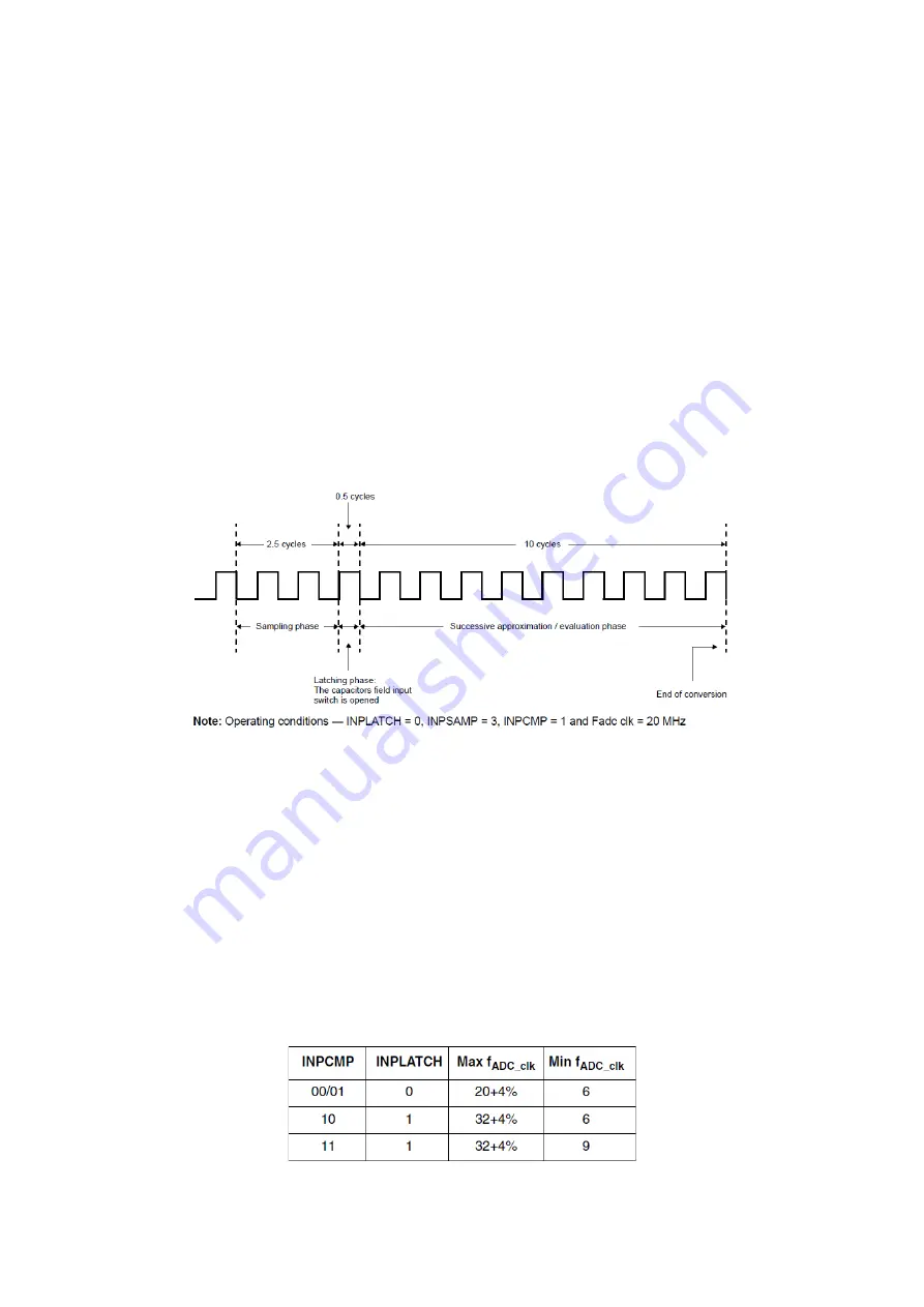
Figure 67 : Sampling and conversion timing example (R.M. Rev8 – Fig. 25-4)
The sampling phase is when the ADC’s internal sampling capacitor is connected to the input pin
and charges up to the input voltage value. This phase’s duration is defined as
𝑇
𝑠𝑎𝑚𝑝𝑙𝑒
=
�
INPSAMP
− 𝑁
𝑑𝑒𝑙𝑎𝑦
�𝑇
𝑐𝑘
, where INPSAMP is configurable, and has to be greater than
or equal to 3,
𝑁
𝑑𝑒𝑙𝑎𝑦
is 0.5 if INPSAMP
≤
6 and 1 otherwise. And
𝑇
𝑠𝑎𝑚𝑝𝑙𝑒
has to be greater than or
equal to 500ns.
𝑇
𝑐𝑘
is the ADC’s clock, derived from the peripheral clock.
The latching phase is when the capacitor’s switch is opened and its duration is
𝑁
𝑑𝑒𝑙𝑎𝑦
𝑇
𝑐𝑘
.
The evaluation phase is the time needed for successive approximation to be performed, its
duration is
𝑇
𝑒𝑣𝑎𝑙
= 10 INPCMP
𝑇
𝑐𝑘
, where INPCMP
≥
1 and INPLATCH < INPCMP. These two
values are configurable, and have to be set using the following table.
Figure 68 : Max/min ADC_clk related to parameters (R.M. Rev8 – Table 25-3)
Содержание MPC5604B
Страница 1: ...LAAS CNRS Quick Start to MPC5604B Embedded Development Sahin Serdar 21 06 2013...
Страница 31: ...Figure 33 INTC SW HW mode comparison Freescale Tutorial...
Страница 87: ......
Страница 132: ......
Страница 133: ...127 Appendix 2 Pad Configurations...
Страница 134: ......
Страница 135: ......
Страница 136: ......
Страница 137: ......
Страница 138: ......
Страница 139: ......
Страница 140: ......
Страница 141: ...Appendix 3 Peripheral input pin selection...
Страница 142: ......
Страница 143: ...137 Appendix 4 Interrupt Vector Table...
Страница 144: ......
Страница 145: ......
Страница 146: ......
Страница 147: ......
Страница 148: ...Appendix 5 I C Baud Rate Prescaler Values...
Страница 149: ......
Страница 150: ......


