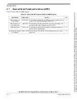


ColdFire Core
MCF52235 ColdFire® Integrated Microcontroller Reference Manual, Rev. 6
3-8
Freescale Semiconductor
3.3
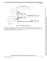
Functional Description
3.3.1
Version 2 ColdFire Microarchitecture
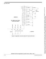
, the non-Harvard architecture of the processor is readily apparent.
The processor interfaces to the local memory subsystem via a single 32-bit address and two unidirectional
32-bit data buses. This structure minimizes the core size without compromising performance to a large
degree.
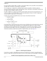
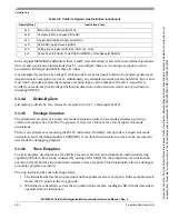
BDM: 0x80E (SR)
Access: Supervisor read/write
BDM read/write
System Byte
Condition Code Register (CCR)
15
14
13
12
11
10
9
8
7
6
5
4
3
2
1
0
R
T
0
S
M
0
I
0
0
0
X
N
Z
V
C
W
Reset
0
0
1
0
0
1
1
1
0
0
0
—
—
—
—
—
Figure 3-8. Status Register (SR)
Table 3-3. SR Field Descriptions
Field
Description
15
T
Trace enable. When set, the processor performs a trace exception after every instruction.
14
Reserved, must be cleared.
13
S
Supervisor/user state.
0 User mode
1 Supervisor mode
12
M
Master/interrupt state. Bit is cleared by an interrupt exception and software can set it during execution of the RTE or
move to SR instructions.
11
Reserved, must be cleared.
10–8
I
Interrupt level mask. Defines current interrupt level. Interrupt requests are inhibited for all priority levels less than or
equal to current level, except edge-sensitive level 7 requests, which cannot be masked.
7–0
CCR
Refer to
Section 3.2.4, “Condition Code Register (CCR)”
.
3.2.8
Memory Base Address Registers (RAMBAR, FLASHBAR)
The memory base address registers are used to specify the base address of the internal SRAM and flash
modules and indicate the types of references mapped to each. Each base address register includes a base
address, write-protect bit, address space mask bits, and an enable bit. FLASHBAR determines the base
address of the on-chip flash, and RAMBAR determines the base address of the on-chip RAM. For more
information, refer to
Section 11.2.1, “SRAM Base Address Register (RAMBAR)”
“Flash Base Address Register (FLASHBAR)”
.
Because
of
an
order
from
the
United
States
International
Trade
Commission,
BGA-packaged
product
lines
and
part
numbers
indicated
here
currently
are
not
available
from
Freescale
for
import
or
sale
in
the
United
States
prior
to
September
2010:MCF52234CVM60,
MCF52235CVM60


