


System Control Module (SCM)
MCF52235 ColdFire® Integrated Microcontroller Reference Manual, Rev. 6
13-4
Freescale Semiconductor
13.5.2
Memory Base Address Register (RAMBAR)
The device supports dual-ported local SRAM memory. This processor-local memory can be accessed
directly by the core and/or other system bus masters. Because this memory provides single-cycle accesses
at processor speed, it is ideal for applications where double-buffer schemes can be used to maximize
system-level performance. For example, a DMA channel in a typical double-buffer application (also
known as a ping-pong scheme) may load data into one portion of the dual-ported SRAM while the
processor is manipulating data in another portion of the SRAM. After the processor completes the data
calculations, it begins processing the recently loaded buffer while the DMA moves out the recently
calculated data from the other buffer, and reloads the next data block into the recently freed memory
region. The process repeats with the processor and the DMA ping-ponging between alternate regions of
the dual-ported SRAM.
The device design implements the dual-ported SRAM in the memory space defined by the RAMBAR
register. There are two physical copies of the RAMBAR register: one located in the processor core and
accessible only via the privileged MOVEC instruction at CPU space address 0xC05 and another located
in the SCM at 0x008. ColdFire core accesses to this memory are controlled by the
processor-local copy of the RAMBAR, while module accesses are enabled by the SCM's RAMBAR.
The physical base address programmed in both copies of the RAMBAR is typically the same value;
however, they can be programmed to different values. By definition, the base address must be a
0-modulo-size value.
IPSBAR
Offset:
0x000 (IPSBAR)
Access: read/write
31
30
29
28
27
26
25
24
23
22
21
20
19
18
17
16
R
BA31 BA30
0
0
0
0
0
0
0
0
0
0
0
0
0
0
W
Reset
0
1
0
0
0
0
0
0
0
0
0
0
0
0
0
0
15
14
13
12
11
10
9
8
7
6
5
4
3
2
1
0
R
0
0
0
0
0
0
0
0
0
0
0
0
0
0
0
V
W
Reset
0
0
0
0
0
0
0
0
0
0
0
0
0
0
0
1
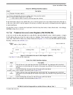
Figure 13-1. IPS Base Address Register (IPSBAR)
Table 13-2. IPSBAR Field Description
Field
Description
31–30
BA
Base address. Defines the base address of the 1-Gbyte internal peripheral space. This is the starting address for the
IPS registers when the valid bit is set.
29–1
Reserved, should be cleared.
0
V
Valid. Enables/disables the IPS Base address region. V is set at reset.
0 IPS Base address is not valid.
1 IPS Base address is valid.
Because
of
an
order
from
the
United
States
International
Trade
Commission,
BGA-packaged
product
lines
and
part
numbers
indicated
here
currently
are
not
available
from
Freescale
for
import
or
sale
in
the
United
States
prior
to
September
2010:MCF52234CVM60,
MCF52235CVM60


