


Static RAM (SRAM)
11-3
Freescale Semiconductor
MCF52235 ColdFire® Integrated Microcontroller Reference Manual, Rev. 6
11.3
Initialization/Application Information
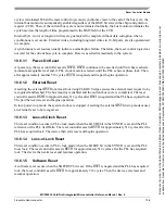
After a hardware reset, the SRAM module contents are undefined. The valid bit of the RAMBAR is
cleared, disabling the processor port into the memory. If the SRAM requires initialization with instructions
or data, perform the following steps:
1. Load the RAMBAR, mapping the SRAM module to the desired location within the address space.
11–10
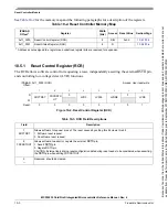
PRIU
PRIL
Priority Bit. PRIU determines if /FEC or CPU has priority in the upper 16K bank of memory. PRIL
determines if DMA/FEC or CPU has priority in the lower 16K bank of memory. If a bit is set, the CPU has
priority. If a bit is cleared, DMA/FEC has priority. Priority is determined according to the following table:
Note: The recommended setting (maximum performance) for the priority bits is 00.
9
SPV
Secondary port valid. Allows access by DMA and FEC.
0 DMA and FEC access to memory is disabled.
1 DMA and FEC access to memory is enabled.
Note: The SPV bit in the second RAMBAR register must also be set to allow dual port access to the SRAM.
For more information, see
Section 10.5.2, “Memory Base Address Register (RAMBAR).”
8
WP
Write Protect. Allows only read accesses to the SRAM. When this bit is set, any attempted write access
from the core generates an access error exception to the ColdFire processor core.
0 Allows core reaought d and write accesses to the SRAM module
1 Allows only core read accesses to the SRAM module
Note: This bit does not affect non-core write accesses.
7–6
Reserved, must be cleared.
5–1
C/I, SC, SD, UC,
UD
Address Space Masks (ASn). These five bit fields allow types of accesses to be masked or inhibited from
accessing the SRAM module. The address space mask bits are:
C/I = CPU space/interrupt acknowledge cycle mask
SC = Supervisor code address space mask
SD = Supervisor data address space mask
UC = User code address space mask
UD = User data address space mask
For each address space bit:
0 An access to the SRAM module can occur for this address space
1 Disable this address space from the SRAM module. If a reference using this address space is made, it
is inhibited from accessing the SRAM module and is processed like any other non-SRAM reference.
These bits are useful for power management as detailed in
Section 11.3.2, “Power Management.”
In most
applications, the C/I bit is set
0
V
Valid. When set, this bit enables the SRAM module; otherwise, the module is disabled. A hardware reset
clears this bit.
0 Contents of RAMBAR are not valid
1 Contents of RAMBAR are valid
Table 11-2. RAMBAR Field Descriptions (continued)
Field
Description
PRIU,PRIL
Upper Bank Priority
Lower Bank Priority
00
DMA/FEC
DMA/FEC
01
DMA/FEC
CPU
10
CPU
DMA/FEC
11
CPU
CPU
Because
of
an
order
from
the
United
States
International
Trade
Commission,
BGA-packaged
product
lines
and
part
numbers
indicated
here
currently
are
not
available
from
Freescale
for
import
or
sale
in
the
United
States
prior
to
September
2010:MCF52234CVM60,
MCF52235CVM60


