


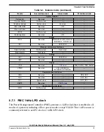

Table 4-1. System memory map (continued)
System 32-bit address range
Destination slave
Access
0xF000_2000–0xF000_2FFF
ROM table
Cortex-M0+ core
0xF000_3000–0xF000_3FFF
Miscellaneous Control Module (MCM)
Cortex-M0+ core
0xF000_4000–0xF7FF_FFFF
Reserved
–
0xF800_0000–0xFFFF_FFFF
IOPORT: GPIO (single cycle)
Cortex-M0+ core
1. The program flash always begins at 0x0000_0000 but the end of implemented flash varies depending on the amount of
flash implemented for a particular device. See
for details.
2. This range varies depending on SRAM sizes. See
for details.
3. Includes BME operations to GPIO at slot 15 (based at 0x4000_F000).
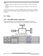
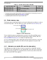
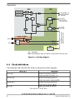
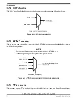
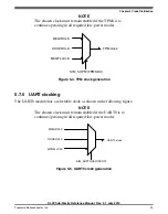
4.3 Flash memory map
The flash memory and the flash registers are located at different base addresses as shown
in the following figure. The base address for each is specified in
Flash
Flash configuration field
Flash base address
Flash memory base address
Registers
Figure 4-1. Flash memory map
The on-chip flash memory is implemented in a portion of the allocated Flash range to
form a contiguous block in the memory map beginning at address 0x0000_0000. See
for details of supported ranges.
Access to the flash memory ranges outside the amount of flash on the device causes the
bus cycle to be terminated with an error followed by the appropriate response in the
requesting bus master.
4.3.1 Alternate non-volatile IRC user trim description
The following non-volatile locations (4 bytes) are reserved for custom IRC user trim
supported by some development tools. An alternate IRC trim to the factory loaded trim
can be stored at this location. To override the factory trim, the user software must load
new values into the MCG trim registers.
Flash memory map
KL02 Sub-Family Reference Manual, Rev. 2.1, July 2013
78
Freescale Semiconductor, Inc.
Содержание KKL02Z32CAF4R
Страница 2: ...KL02 Sub Family Reference Manual Rev 2 1 July 2013 2 Freescale Semiconductor Inc...
Страница 24: ...KL02 Sub Family Reference Manual Rev 2 1 July 2013 24 Freescale Semiconductor Inc...
Страница 36: ...Orderable part numbers KL02 Sub Family Reference Manual Rev 2 1 July 2013 36 Freescale Semiconductor Inc...
Страница 76: ...Human machine interfaces HMI KL02 Sub Family Reference Manual Rev 2 1 July 2013 76 Freescale Semiconductor Inc...
Страница 94: ...Module clocks KL02 Sub Family Reference Manual Rev 2 1 July 2013 94 Freescale Semiconductor Inc...
Страница 142: ...Functional description KL02 Sub Family Reference Manual Rev 2 1 July 2013 142 Freescale Semiconductor Inc...
Страница 188: ...Memory map and register descriptions KL02 Sub Family Reference Manual Rev 2 1 July 2013 188 Freescale Semiconductor Inc...
Страница 214: ...Application information KL02 Sub Family Reference Manual Rev 2 1 July 2013 214 Freescale Semiconductor Inc...
Страница 222: ...Memory map register descriptions KL02 Sub Family Reference Manual Rev 2 1 July 2013 222 Freescale Semiconductor Inc...
Страница 256: ...Memory map and register definition KL02 Sub Family Reference Manual Rev 2 1 July 2013 256 Freescale Semiconductor Inc...
Страница 300: ...Functional description KL02 Sub Family Reference Manual Rev 2 1 July 2013 300 Freescale Semiconductor Inc...
Страница 532: ...Functional description KL02 Sub Family Reference Manual Rev 2 1 July 2013 532 Freescale Semiconductor Inc...
Страница 534: ...KL02 Sub Family Reference Manual Rev 2 1 July 2013 534 Freescale Semiconductor Inc...


