


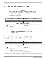


GPIOx_PDDR field descriptions (continued)
Field
Description
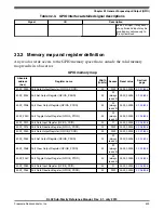
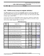
32.3 FGPIO memory map and register definition
The GPIO registers are also aliased to the IOPORT interface on the Cortex-M0+ from
address 0xF800_0000. Accesses via the IOPORT interface occur in parallel with any
instruction fetches and will therefore complete in a single cycle. This aliased Fast GPIO
memory map is called FGPIO.
Any read or write access to the FGPIO memory space that is outside the valid memory
map results in a bus error. All register accesses complete with zero wait states, except
error accesses which complete with one wait state.
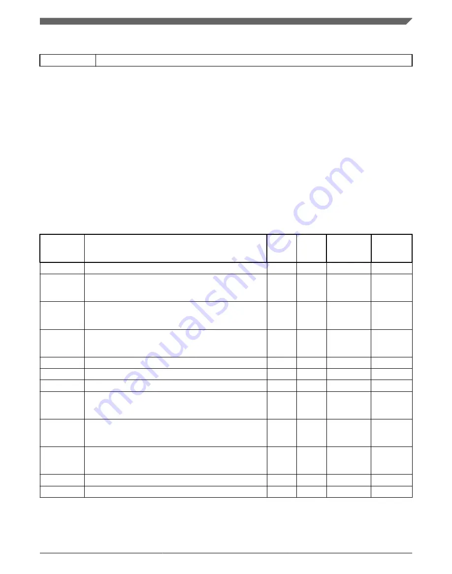
FGPIO memory map
Absolute
address
(hex)
Register name
Width
(in bits)
Access Reset value
Section/
page
F800_0000 Port Data Output Register (FGPIOA_PDOR)
32
R/W
0000_0000h
F800_0004 Port Set Output Register (FGPIOA_PSOR)
32
W
(always
reads 0)
0000_0000h
F800_0008 Port Clear Output Register (FGPIOA_PCOR)
32
W
(always
reads 0)
0000_0000h
F800_000C Port Toggle Output Register (FGPIOA_PTOR)
32
W
(always
reads 0)
0000_0000h
F800_0010 Port Data Input Register (FGPIOA_PDIR)
32
R
0000_0000h
F800_0014 Port Data Direction Register (FGPIOA_PDDR)
32
R/W
0000_0000h
F800_0040 Port Data Output Register (FGPIOB_PDOR)
32
R/W
0000_0000h
F800_0044 Port Set Output Register (FGPIOB_PSOR)
32
W
(always
reads 0)
0000_0000h
F800_0048 Port Clear Output Register (FGPIOB_PCOR)
32
W
(always
reads 0)
0000_0000h
F800_004C Port Toggle Output Register (FGPIOB_PTOR)
32
W
(always
reads 0)
0000_0000h
F800_0050 Port Data Input Register (FGPIOB_PDIR)
32
R
0000_0000h
F800_0054 Port Data Direction Register (FGPIOB_PDDR)
32
R/W
0000_0000h
Chapter 32 General-Purpose Input/Output (GPIO)
KL02 Sub-Family Reference Manual, Rev. 2.1, July 2013
Freescale Semiconductor, Inc.
527
Содержание KKL02Z32CAF4R
Страница 2: ...KL02 Sub Family Reference Manual Rev 2 1 July 2013 2 Freescale Semiconductor Inc...
Страница 24: ...KL02 Sub Family Reference Manual Rev 2 1 July 2013 24 Freescale Semiconductor Inc...
Страница 36: ...Orderable part numbers KL02 Sub Family Reference Manual Rev 2 1 July 2013 36 Freescale Semiconductor Inc...
Страница 76: ...Human machine interfaces HMI KL02 Sub Family Reference Manual Rev 2 1 July 2013 76 Freescale Semiconductor Inc...
Страница 94: ...Module clocks KL02 Sub Family Reference Manual Rev 2 1 July 2013 94 Freescale Semiconductor Inc...
Страница 142: ...Functional description KL02 Sub Family Reference Manual Rev 2 1 July 2013 142 Freescale Semiconductor Inc...
Страница 188: ...Memory map and register descriptions KL02 Sub Family Reference Manual Rev 2 1 July 2013 188 Freescale Semiconductor Inc...
Страница 214: ...Application information KL02 Sub Family Reference Manual Rev 2 1 July 2013 214 Freescale Semiconductor Inc...
Страница 222: ...Memory map register descriptions KL02 Sub Family Reference Manual Rev 2 1 July 2013 222 Freescale Semiconductor Inc...
Страница 256: ...Memory map and register definition KL02 Sub Family Reference Manual Rev 2 1 July 2013 256 Freescale Semiconductor Inc...
Страница 300: ...Functional description KL02 Sub Family Reference Manual Rev 2 1 July 2013 300 Freescale Semiconductor Inc...
Страница 532: ...Functional description KL02 Sub Family Reference Manual Rev 2 1 July 2013 532 Freescale Semiconductor Inc...
Страница 534: ...KL02 Sub Family Reference Manual Rev 2 1 July 2013 534 Freescale Semiconductor Inc...


