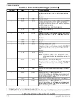


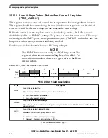

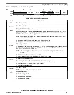
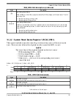
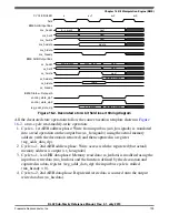
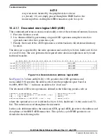
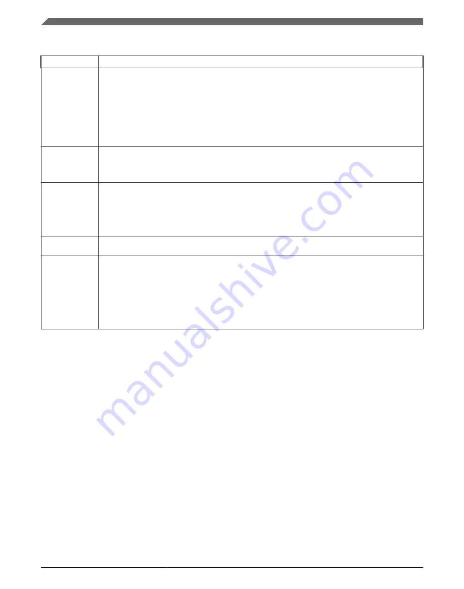
PMC_LVDSC2 field descriptions
Field
Description
7
LVWF
Low-Voltage Warning Flag
This read-only status bit indicates a low-voltage warning event. LVWF is set when V
Supply
transitions below
the trip point, or after reset and V
Supply
is already below V
LVW
. LVWF bit may be 1 after power on reset,
therefore, to use LVW interrupt function, before enabling LVWIE, LVWF must be cleared by writing
LVWACK first.
0
Low-voltage warning event not detected
1
Low-voltage warning event detected
6
LVWACK
Low-Voltage Warning Acknowledge
This write-only bit is used to acknowledge low voltage warning errors. Write 1 to clear LVWF. Reads
always return 0.
5
LVWIE
Low-Voltage Warning Interrupt Enable
Enables hardware interrupt requests for LVWF.
0
Hardware interrupt disabled (use polling)
1
Request a hardware interrupt when LVWF = 1
4–2
Reserved
This field is reserved.
This read-only field is reserved and always has the value 0.
LVWV
Low-Voltage Warning Voltage Select
Selects the LVW trip point voltage (V
LVW
). The actual voltage for the warning depends on LVDSC1[LVDV].
00
Low trip point selected (V
LVW
= V
LVW1
)
01
Mid 1 trip point selected (V
LVW
= V
LVW2
)
10
Mid 2 trip point selected (V
LVW
= V
LVW3
)
11
High trip point selected (V
LVW
= V
LVW4
)
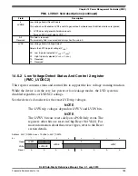
14.5.3 Regulator Status And Control register (PMC_REGSC)
The PMC contains an internal voltage regulator. The voltage regulator design uses a
bandgap reference that is also available through a buffer as input to certain internal
peripherals, such as the CMP and ADC. The internal regulator provides a status bit
(REGONS) indicating the regulator is in run regulation.
NOTE
This register is reset on Chip Reset Not VLLS and by reset
types that trigger Chip Reset not VLLS. See the Reset section
details for more information.
Memory map and register descriptions
KL02 Sub-Family Reference Manual, Rev. 2.1, July 2013
186
Freescale Semiconductor, Inc.
Содержание KKL02Z32CAF4R
Страница 2: ...KL02 Sub Family Reference Manual Rev 2 1 July 2013 2 Freescale Semiconductor Inc...
Страница 24: ...KL02 Sub Family Reference Manual Rev 2 1 July 2013 24 Freescale Semiconductor Inc...
Страница 36: ...Orderable part numbers KL02 Sub Family Reference Manual Rev 2 1 July 2013 36 Freescale Semiconductor Inc...
Страница 76: ...Human machine interfaces HMI KL02 Sub Family Reference Manual Rev 2 1 July 2013 76 Freescale Semiconductor Inc...
Страница 94: ...Module clocks KL02 Sub Family Reference Manual Rev 2 1 July 2013 94 Freescale Semiconductor Inc...
Страница 142: ...Functional description KL02 Sub Family Reference Manual Rev 2 1 July 2013 142 Freescale Semiconductor Inc...
Страница 188: ...Memory map and register descriptions KL02 Sub Family Reference Manual Rev 2 1 July 2013 188 Freescale Semiconductor Inc...
Страница 214: ...Application information KL02 Sub Family Reference Manual Rev 2 1 July 2013 214 Freescale Semiconductor Inc...
Страница 222: ...Memory map register descriptions KL02 Sub Family Reference Manual Rev 2 1 July 2013 222 Freescale Semiconductor Inc...
Страница 256: ...Memory map and register definition KL02 Sub Family Reference Manual Rev 2 1 July 2013 256 Freescale Semiconductor Inc...
Страница 300: ...Functional description KL02 Sub Family Reference Manual Rev 2 1 July 2013 300 Freescale Semiconductor Inc...
Страница 532: ...Functional description KL02 Sub Family Reference Manual Rev 2 1 July 2013 532 Freescale Semiconductor Inc...
Страница 534: ...KL02 Sub Family Reference Manual Rev 2 1 July 2013 534 Freescale Semiconductor Inc...


