Reproduction forbidden without Fibocom Wireless Inc. written authorization - All Rights Reserved.
FIBOCOM SU806 Series Hardware Guide
Page 51 of 91
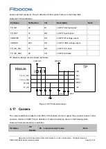
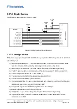
3.17.3 Depth Camera
Pin definition of depth camera is shown as follow:
Module
MIPI_CSI1_LN3_P
DCAM_RST
MIPI_CSI1_LN3_N
MIPI_CSI1_LN2_P
MIPI_CSI1_LN2_N
CAM_I2C_SDA1
CAM_I2C_SCL1
DCAM_PWDN
DCAM_MCLK
CLK_P
MCLK
CLK_N
DAT0_P
DAT0_N
C
A
M
C
on
ne
ct
or
PWD
RST
SCL
SDA
VDD1V85
NC
NC
VDDCAMA
AVDD
DOVDD
VDD1V8
EMI
EMI
10
uF
1
0
0
nF
1
uF
Figure 3-19 Depth camera reference design
3.17.4 Design Notice
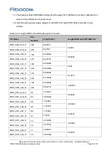
MIPI_CSI is a high-speed signal which has relatively high requirement for routing and must be prioritized
when PCB layout.
1) MIPI is a high-speed signal. It is recommended to connect the common mode inductor in series
near the LCD connector to reduce the electromagnetic interference of the circuit.
2) MIPI routing is recommended to be in the inner layer, with three-dimensional grounding;
3) The MIPI signal needs to be controlled with a differential impedance of 100
Ω tolerance ±10%;
4) The total length of the
trace must ≤ 70mm, VIAs ≤ 4;
5) The intra lane match of MIPI
differential pair signal must ≤ 0.5mm;
6) The inter lane match of MIPI
signal must ≤ 2mm;
7) It is recommended that the space of intra lane should be 1.5 times trace width and the differential
cable should keep 3 times trace width from other cable;
8) The parasitic capacitance of differential signal must not exceed 1.0pF;
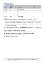
The matters need attention of another camera signal:
9) CAM_CLK is a high-speed clock signal and requires three-dimensional grounding
10) If two cameras share the same I2C interface, please confirm the I2C addresses of the two
cameras do not conflict;

