


FDA-2A Manual.doc
Rev. 1.0
Page 1
31-Aug-2012
www.FETAudio.com
FDA-2A Manual
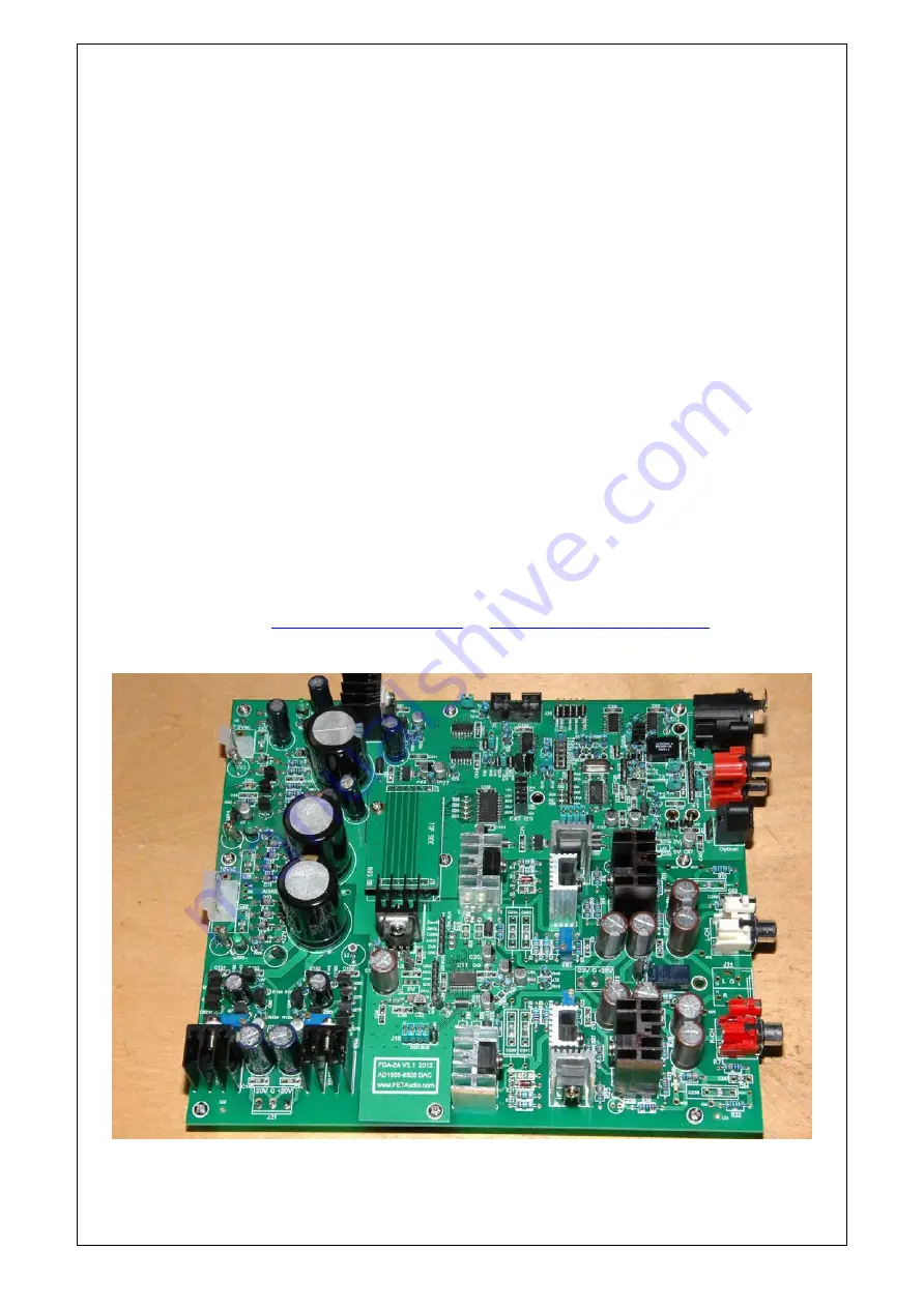
WM8805 Single Ended DAC
~~~~~~~~~~~~~~~~~~~~~~~~~~~~~~~~~~~~~~~~
High Fidelity 24 bit*192kS/s
Digital to Analogue Converter
~~~~~~~~~~~~~~~~~~~~~~~~~~~~~~~~~~~~~~~~
Designed By Spencer Cheung of FETAudio.com
or
www.FETAudio.com
Содержание FDA-2A
Страница 38: ...w w w F E T A u d i o c o m w w w F E T A u d i o c o m ...
Страница 39: ...w w w F E T A u d i o c o m w w w F E T A u d i o c o m ...
Страница 40: ...w w w F E T A u d i o c o m ...