2007-11-19
Page 26 of 35
IT321_Tech_doc_12
6. REFERENCE
DESIGN
The idea of the reference design is to give a guideline for the applica-
tions using the OEM GPS module. In itself it is not a finished product,
but an example that performs correctly.
In the following two chapters the reader is exposed to design rules
that he should follow, when designing the GPS receiver in to the ap-
plication. By following the rules one end up having an optimal design
with no unexpected behavior caused by the PCB layout itself. In fact
these guidelines are quite general in nature, and can be utilized in
any PCB design related to RF techniques or to high speed logic.
6.1 Reference circuit diagram
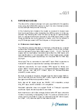
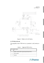
The following picture describes a minimum connectivity for a typical
autonomous navigation application. It consists of the IT321 module,
which is powered by the main VDD supply (+3.3V… +5.5V). The VDD
supply can be raw battery connection given that the VDD ripple volt-
age specification is not exceeded. With a high ripple power supply
use an external by-pass capacitor(s) or a low pass filter for VDD sup-
ply input.
Serial port TXA is connected to host UART input. RXA connection to
host UART output is required when sending commands to IT321.
Optional connectivity for host includes PPS signal for timing pur-
poses, BOOT control inputs for e.g. re-programming the firmware with
flash version and ON_OFF control input for Normal/Hibernate
(ON/OFF) mode control.
No back up supply is required. Instead keep the main supply VDD ac-
tive all the time and use the ON_OFF control input to switch between
Navigation and Hibernate operation mode.
Note that all I/O signal levels are CMOS 1.8V compatible, except
ON_OFF input, which is CMOS 1.2V compatible.
Standard operation does not support ELCK or Timesync operation
and these inputs should be pulled to low state.
Note that there is a DC bias voltage present at the RF input, when the
module is operating in Navigating mode. If a passive antenna with a
short-circuit to the GND is used, an external series DC block capaci-
tor (18pF…1nF) must be used for the antenna input.
Содержание IT321
Страница 15: ...2007 11 19 Page 15 of 35 IT321_Tech_doc_12 Figure 2 SiRFFlash utility settings...
Страница 25: ...2007 11 19 Page 25 of 35 IT321_Tech_doc_12 Figure 7 Tape and reel specification...
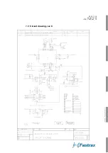
Страница 32: ...2007 11 19 Page 32 of 35 IT321_Tech_doc_12 7 3 Circuit drawing rev C...
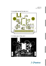
Страница 33: ...2007 11 19 Page 33 of 35 IT321_Tech_doc_12 7 4 Assembly drawing Top side rev C 7 5 Artwork layer 1 Top rev C...
Страница 34: ...2007 11 19 Page 34 of 35 IT321_Tech_doc_12 7 6 Artwork layer 2 rev C 7 7 Artwork layer 3 rev C...
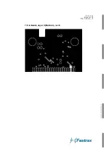
Страница 35: ...2007 11 19 Page 35 of 35 IT321_Tech_doc_12 7 8 Artwork layer 4 Bottom rev C...

