12 SYNCHRONOUS SERIAL INTERFACE (SPIA)
S1C17M12/M13 TECHNICAL MANUAL
Seiko Epson Corporation
12-7
(Rev. 1.2)
12.5.3 Data Reception in Master Mode
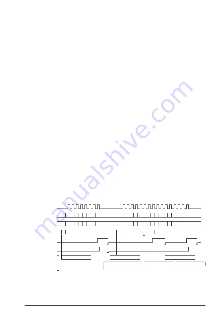
A data receiving procedure and operations in master mode are shown below. Figures 12.5.3.1 and 12.5.3.2 show a
timing chart and flowcharts, respectively.
Data receiving procedure
1. Assert the slave select signal by controlling the general-purpose output port (if necessary).
2. Check to see if the SPI
n
INTF.TBEIF bit is set to 1 (transmit buffer empty).
3. Write dummy data (or transmit data) to the SPI
n
TXD register.
4. Wait for a transmit buffer empty interrupt (SPI
n
INTF.TBEIF bit = 1).
5. Write dummy data (or transmit data) to the SPI
n
TXD register.
6. Wait for a receive buffer full interrupt (SPI
n
INTF.RBFIF bit = 1).
7. Read the received data from the SPI
n
RXD register.
8. Repeat Steps 5 to 7 until the end of data reception.
9. Negate the slave select signal by controlling the general-purpose output port (if necessary).
Note: To perform continuous data reception without stopping SPICLKn, Steps 7 and 5 operations must
be completed within the SPICLKn cycles equivalent to “Data bit length - 1” after Step 6.
Data receiving operations
SPIA Ch.
n
starts data receiving operations simultaneously with data sending operations when transmit data (may
be dummy data if data transmission is not required) is written to the SPI
n
TXD register.
The SPICLK
n
pin outputs clocks of the number of the bits specified by the SPI
n
MOD.CHLN[3:0] bits. The
transmit data bits are output in sequence from the SDO
n
pin in sync with these clocks and the receive data bits
input from the SDI
n
pin are shifted into the shift register.
When the last clock is output from the SPICLK
n
pin and receive data bits are all shifted into the shift register,
the received data is transferred to the receive data buffer and the SPI
n
INTF.RBFIF bit is set to 1. At the same
time SPIA issues a receive buffer full interrupt request if the SPI
n
INTE.RBFIE bit = 1. After that, the received
data in the receive data buffer can be read through the SPI
n
RXD register.
Note: If data of the number of the bits specified by the SPInMOD.CHLN[3:0] bits is received when the
SPInINTF.RBFIF bit is set to 1, the SPInRXD register is overwritten with the newly received data
and the previously received data is lost. In this case, the SPInINTF.OEIF bit is set.
SPICLKn
SDOn
SDIn
SPInINTF.TBEIF
SPInINTF.RBFIF
SPInINTF.TENDIF
Software operations
1 2 3 4 5 6 7 8
1 2 3 4 5 6 7 8 1 2 3 4 5 6 7 8
Data (W)
→
SPInTXD
Data (W)
→
SPInTXD
Data (W)
→
SPInTXD
SPInRXD
→
Data (R)
1 (W)
→
SPInINTF.TENDIF
SPInRXD
→
Data (R)
SPInRXD
→
Data (R)
Figure 12.5.3.1 Example of Data Receiving Operations in Master Mode (SPInMOD.CHLN[3:0] bits = 0x7)


