18 uaRT
S1C17624/604/622/602/621 TeChniCal Manual
Seiko epson Corporation
18-3
Stop bit
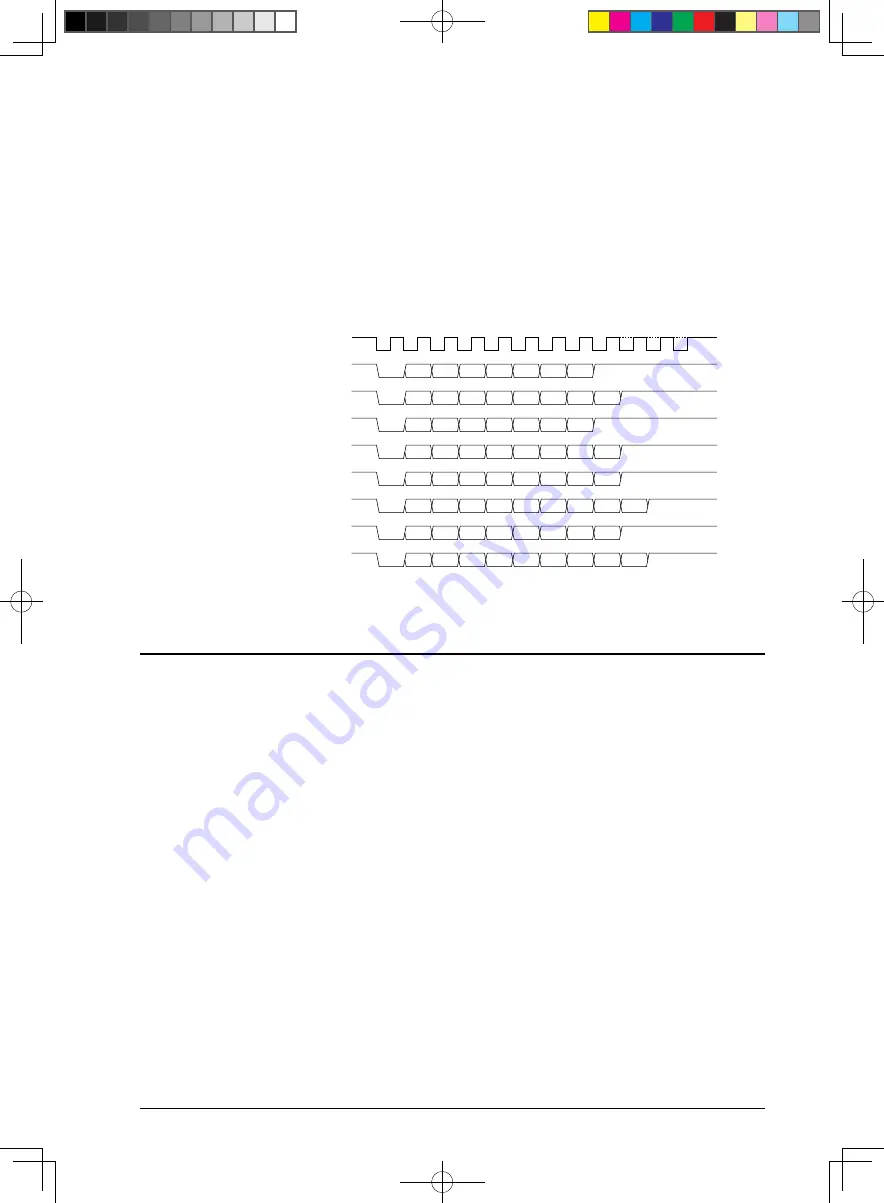
The stop bit length is selected by STPB/UART_MOD
x
register. Setting STPB to 0 (default) configures the stop
bit length to 1 bit. Setting STPB to 1 configures it to 2 bits.
Parity bit
Whether the parity function is enabled or disabled is selected by PREN/UART_MOD
x
register. Setting PREN
to 0 (default) disables the parity function. In this case, no parity bit is added to the transfer data and the data is
not checked for parity when received. Setting PREN to 1 enables the parity function. In this case, a parity bit is
added to the transfer data and the data is checked for parity when received. When the parity function is enabled,
the parity mode is selected by PMD/UART_MOD
x
register. Setting PMD to 0 (default) adds a parity bit and
checks for even parity. Setting PMD to 1 adds a parity bit and checks for odd parity.
Sampling clock (sclk)
CHLN = 0, PREN = 0, STPB = 0
CHLN = 0, PREN = 1, STPB = 0
CHLN = 0, PREN = 0, STPB = 1
CHLN = 0, PREN = 1, STPB = 1
CHLN = 1, PREN = 0, STPB = 0
CHLN = 1, PREN = 1, STPB = 0
CHLN = 1, PREN = 0, STPB = 1
CHLN = 1, PREN = 1, STPB = 1
s1
D0
D1
D2
D3
D4
D5
D6
s2
s1
D0
D1
D2
D3
D4
D5
D6
p
s2
s1
D0
D1
D2
D3
D4
D5
D6
s2
s3
s1
D0
D1
D2
D3
D4
D5
D6
p
s2
s3
s1
D0
D1
D2
D3
D4
D5
D6
D7
s2
s1
D0
D1
D2
D3
D4
D5
D6
D7
p
s2
s1
D0
D1
D2
D3
D4
D5
D6
D7
s2
s3
s1
D0
D1
D2
D3
D4
D5
D6
D7
p
s2
s3
s1: start bit, s2 & s3: stop bit, p: parity bit
Figure 18.4.1 Transfer Data Format
Data Transfer Control
18.5
Make the following settings before starting data transfers.
(1) Select the input clock. (See Section 18.3.)
Program T8F to output the transfer clock.
(2) Set the transfer data format. (See Section 18.4.)
(3) To use the IrDA interface, set IrDA mode. (See Section 18.8.)
(4) Set interrupt conditions to use UART interrupts. (See Section 18.7.)
note: Make sure the UART is halted (RXEN/UART_CTL
x
register = 0) before changing the above set-
tings.
enabling data transfers
Set RXEN/UART_CTL
x
register to 1 to enable data transfers. This puts the transmitter/receiver circuit in ready-
to-transmit/receive status.
note: Do not set RXEN to 0 while the UART is sending or receiving data.
Data transmission control
To start data transmission, write the transmit data to TXD[7:0]/UART_TXD
x
register.
The data is written to the transmit data buffer, and the transmitter circuit starts sending data.
The buffer data is sent to the transmit shift register, and the start bit is output from the SOUT
x
pin. The data in
the shift register is then output from the LSB. The transfer data bit is shifted in sync with the sampling clock
rising edge and output in sequence via the SOUT
x
pin. Following output of MSB, the parity bit (if parity is en-
abled) and the stop bit are output.


