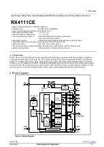


3. Terminal Description
RX4111CE
Jump to
ETM62E-02
Seiko Epson Corporation
6
3. Terminal Description
3.1. Terminal Connections
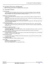
RX4111CE
1. V
DD
10. /INT
2. V
BAT
9. GND
3. DI
8. V
IO
4. FOUT
7. CE
5. CLK
6. DO
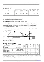
Figure 3 Package Pin Layout
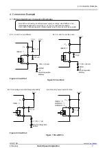
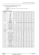
3.2. Pin Functions
Table 1 Pin Description
Signal
name
I/O
Function
CE
Input
Chip enables input pin (SS)
Should be held high to allow access to the CPU.
Incorporates a pull-down resistor
CLK
Input
Serial clock input pin (SCLK)
DI
Input
Data input pin (MOSI)
DO
Output
Data output pin (MISO)
FOUT
Output
Frequency output pin (CMOS)
(frequency selection: 32.768 kHz, 1024 Hz, 1 Hz)
When output is stopped, the FOUT pin is High impedance.
/INT
Open-Drain
Output
This pin is used to output alarm signals, timer signals, time update signals, and other
signals. This pin is an N-ch open drain
V
DD
Power-supply pin
Possible to supply different voltage from V
IO
V
IO
Interface power supply pin
Input to supply the voltage same as a host
V
BAT
This is a power supply pin for backup battery
Connect an EDLC, a secondary battery, a primary battery
In the backup voltage range, supplied to IC, from this pin
GND
Ground pin
Note:
Be sure to connect a bypass capacitor rated at least 0.1 μF between V
DD
and GND.
For the input terminals, it is permitted for the input to be 5.5 V regardless of the V
IO
voltage.
For the Open-Drain pin, it is permitted for the pull-up to be 5.5 V regardless of the V
IO
voltage.
When FOUT or INT is not used, be left open in these pins. It doesn't need pull-Up/Down resistor.


