background image


14. How to use 


RX4111CE 


Jump t

Top 

Bottom


ETM62E-02                                               

Seiko Epson Corporation                                                                   


54


6) 

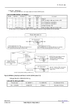
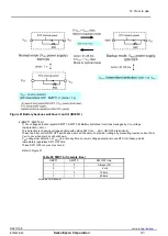
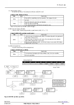
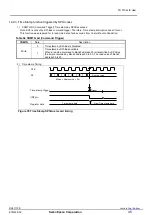
Setting example of the Alarm interrupt function 


Next process 

Fh 




 Select and set /INT output in AIE bit. 


Bank1 - Dh 



 Select week or day in WADA bit. 


Eh 



 Clear AF bit 


Alarm setting 



Set AIE bit to 

“0” to stop Alarm-interrupt function. 




 Set alarm data. 


Bank1 - Fh 

Bank1 - 7h



 9h 

Bank2 - Ch 


                          Figure 45 Flow7 


Содержание RX4111CE

Страница 1: ...Real Time Clock Module RX4111CE Product name Product number RX4111CE A X1B000431000115 RX4111CE B X1B000431000215 Application manual ...

Страница 2: ...d in general electronic applications and specifically designated applications Anticipated Purpose Epson products are NOT intended for any use beyond the Anticipated Purpose that requires particular quality or extremely high reliability in order to refrain from causing any malfunction or failure leading to critical harm to life and health serious property damage or severe impact on society includin...

Страница 3: ...ymbol of tRTN was separated to tRTN1 and tRTN2 35 As for time of auto release of Time update interruption Symbol name was updated to tRTN1 from tRTN The symbol of tRTN was separated to tRTN1 and tRTN2 Auto release time of Time update interruption was corrected 7 324ms to 7 644ms from 7 57 ms 14 4 Time Update Interrupt Function Table 37 UIE bit Update Interrupt Enable 36 Figure 1 Time Update Interr...

Страница 4: ... 1 12 9 2 2 AC Characteristics 2 13 10 Interface timing when power ON OFF 13 10 1 Restrictions of SPI Bus interface in the power ON OFF 13 10 2 VDD and CE Timing at Power On 14 10 3 Reset by Software 15 11 Reference information 16 11 1 Reference Data 16 12 Application notes 17 13 Overview of Functions and Registers 18 13 1 Overview of Functions 18 13 2 Register Table 19 13 2 1 Register Table 19 13...

Страница 5: ...on Diagram 36 14 5 Status Monitoring Function 37 14 5 1 Related Registers For Status Monitoring 37 14 6 FOUT Function Clock Output Function 38 14 6 1 FOUT Control Register 38 14 6 2 FOUT Function Table 38 14 7 Battery Backup Switchover Function 39 14 7 1 Description of Battery Backup Switchover Function 39 14 8 Time Stamp Function 43 14 8 1 Description Of Time Stamp Function 43 14 8 2 Related Regi...

Страница 6: ...or and SPI Bus interface In addition to providing a calendar year month date day hour minute second this module provides other functions including time stamp from 1 1024 second to year alarm wake up timer time update interruption and 32 768 kHz output Time stamp function can record maximum of 8 events Using the backup battery switch control function and the interface power supply input pin RX4111C...

Страница 7: ...pedance INT Open Drain Output This pin is used to output alarm signals timer signals time update signals and other signals This pin is an N ch open drain VDD Power supply pin Possible to supply different voltage from VIO VIO Interface power supply pin Input to supply the voltage same as a host VBAT This is a power supply pin for backup battery Connect an EDLC a secondary battery a primary battery ...

Страница 8: ...t in each of pin as much as possible EX 1 VIO and VDD are different Ex 2 VIO and VDD are the same Figure 4 Circuit Ex 1 Figure 5 Circuit Ex 2 Ex 3 Connecting a Non RE Chargeable battery Ex 4 Not using power switch function Figure 6 Circuit Ex 3 Figure 7 Circuit EX 4 VDD VBAT VIO 1 8 V 3 3 V I V R 40 mA 0 1 F 0 1 F Re chargeable Battery EDLC or INIEN 1 VDD VBAT VIO Non Re chargeable battery 3 3 V I...

Страница 9: ...e of the 1st and 10th pins of the package are inspection pads for the crystal unit For stable oscillation make sure that leakage current due to condensation or dust does not occur between these pads The metal pads on the short side of the 5 pin and 6 pin sides are not connected inside the RTC Figure 8 External dimensions 5 2 Marking Layout RX4111CE 1 Pin Mark Logo Production lot R4111X 123A Freque...

Страница 10: ...f supply Voltage 1 1 V Operating temperature T_use No condensation 40 25 85 C Minimum value of Clock supply voltage VCLK is the lower supply voltage limit till which the RTC can assure the clock to run For proper initialization of the RTC RX4111 it is necessary that VDD voltage exceeds 1 6V at power up 8 Frequency Characteristics Table 4 Frequency Characteristics Unless otherwise specified VBAT VD...

Страница 11: ...ltage of VBAT from VDD 1 20 1 30 1 40 V High Input voltage VIH CE CLK DI 0 8 VIO 5 5 V Low Input voltage VIL CE CLK DI GND 0 3 0 2 VIO V High Output voltage VOH1 FOUT DO VIO 5 0 V IOH 1 mA 4 5 5 0 V VOH2 VIO 3 0 V IOH 1 mA 2 2 3 0 VOH3 VIO 3 0 V IOH 100 A 2 9 3 0 Low Output voltage VOL1 FOUT DO VIO 5 0 V IOL 1 mA GND GND 0 5 V VOL2 VIO 3 0 V IOL 1 mA GND GND 0 8 VOL3 VIO 3 0 V IOL 100 A GND GND 0 ...

Страница 12: ...BAT Vertical Axis Charge current Ichg Figure 10 Chargeable current of VBAT VDD 3 0 V Figure 11 Chargeable Current of VBAT VDD 5 5V Figure 12 Circuit of charge to Re chargeable Battery 9 1 3 Reference Value of Switching Element Table 6 Reference value of switching element Item Characteristics Condition Current tolerance 40 mA Max SW ON 25 C Diode Vf 0 60 V 1 mA Typ 0 85 V 10 mA Typ VDD 3 0 V 25 C D...

Страница 13: ...data setup time tDS 200 50 40 ns Write data hold time tDH 200 50 40 ns Read data delay time tRD CL 50 pF 0 400 150 110 ns DO output disable time tRZ CL 50 pF RL 10 k 0 400 120 110 ns DI DO conflict avoiding time tZZ 0 0 0 ns 1 Please refer to a standard of VIO 1 8 V 0 2 V for VIO 2 0 V 2 7 V 2 Please refer to a standard of VIO 3 0 V 10 for VIO 3 3 V 4 5 V Timing chart CLK C E tCLKS tWH tWL tCH tCR...

Страница 14: ...s or more VDD VBAT 3 VCLK GND Power supply VDD VBAT tR1 VDET 1 Backup mode tCL 2 tCU VDET VDET SPI Access is enabled VBAT Access is disabled VDD Access is enabled Figure 14 Power on Sequence Table 9 Power up down characteristics Item Symbol Condition Min Typ Max Unit Initial power supply rise time tR1 From GND to VDD VDET1 5 V 0 1 10 ms V 3 V 0 5 10 ms V Access wait time Initial power on tCL After...

Страница 15: ... the built in crystal oscillator the RTC does not work normally without the integrated oscillator having stabilized Please initialize the RTC at the time the power supply voltage returns VLF 1 after the oscillation has stabilized after oscillation start time t_STA If intending to access the RTC after the main supply voltage returns please note following points VDD VDD detect voltage VDET Internal ...

Страница 16: ...b 6 Write 80h Address Bank3 Fh TEST 1 3 7 Write 6Ch Address Bank5 0h 8 Write 03h Address Bank5 1h 9 Write 10h Address Bank5 2h 10 Write 20h Address Bank5 3h 11 Wait more than 2 ms TEST bit is reset automatically 4 1 1 When 40 ms waiting time is so long time in your system an another method Jump to step3 from step1 At step4 when VLF is 1 write 0 to VLF While VLF is 1 repeat reset to VLF and verify ...

Страница 17: ...condary temperature 0 035 0 005 10 6 C2 T C Ultimate temperature 25 5 C X C Any temperature 2 To determine overall clock accuracy add the frequency precision and voltage characteristics f f f fo fT fV f f Clock accuracy stable frequency in any temperature and voltage f fo Frequency precision fT Frequency deviation in any temperature fV Frequency deviation in any voltage 3 How to find the date diff...

Страница 18: ...causes increase of a consumption electric current and the behavior that are instability Please connect an unused input terminal to VIO or GND 2 Notes on packaging 1 Soldering heat resistance If the temperature within the package exceeds 260 C the characteristics of the crystal oscillator will be degraded and it may be damaged The reflow conditions within our reflow profile is recommended Therefore...

Страница 19: ...automatically sum them up 3 Alarm Interrupt Function The alarm interrupt function generates interrupt events for alarm settings such as date day hour minute and second settings When an interrupt event occurs the AF bit value is set to 1 and the INT pin goes to low level to indicate that an event has occurred 4 Voltage Drop Detection Function This is a function to detect a drop in VDD voltage It is...

Страница 20: ... 0 128 64 32 16 8 4 2 1 Bh Timer Counter 1 32768 16384 8192 4096 2048 1024 512 256 Ch Timer Counter 2 8388608 4194304 2097152 1048576 524288 262144 131072 65536 Dh Extension Register FSEL1 FSEL0 USEL TE WADA TSEL1 TSEL0 Eh Flag Register POR z UF TF AF EVF VLF XST Fh Control Register z z UIE TIE AIE EIE z STOP Bank2 Function bit 7 bit 6 bit 5 bit 4 bit 3 bit 2 bit 1 bit 0 Address 0h Time Stamp 1 10...

Страница 21: ...0 10 8 4 2 1 Ch Time Stamp DAY 20 10 8 4 2 1 Dh Time Stamp MONTH 10 8 4 2 1 Eh Time Stamp YEAR 80 40 20 10 8 4 2 1 Fh Status stamp VDET XST After the initial power up from 0 V or in case the VLF bit returns 1 make sure to initialize all registers before using the RTC Be sure to avoid entering incorrect date and time data as clock operations are not guaranteed when the data or time data is incorrec...

Страница 22: ...WEEK Alarm 1 X X X X X X X DAY Alarm X X X X X X X Ah Timer Counter 0 X X X X X X X X Bh Timer Counter 1 X X X X X X X X Ch Timer Counter 2 X X X X X X X X Dh Extension Register 0 0 0 0 0 0 1 0 Eh Flag Register 1 0 0 0 0 0 1 X Fh Control Register 0 0 0 0 0 0 0 0 Bank 2 Address Function bit 7 bit 6 bit 5 bit 4 bit 3 bit 2 bit 1 bit 0 0h Time Stamp 1 1024S 0 0 0 0 X X X X 1h Time Stamp 1 256S X X X ...

Страница 23: ... Eh No Function X X X X X X X X Fh TEST 0 0 0 0 0 0 0 0 Bank4 5 6 7 Address Function bit 7 bit 6 bit 5 bit 4 bit 3 bit 2 bit 1 bit 0 0h Time stamp 1 256S X X X X X X X X 1h Time Stamp SEC X X X X X X X X 2h Time Stamp MIN X X X X X X X X 3h Time Stamp HOUR X X X X X X X X 7h Time Stamp DAY X X X X X X X X 5h Time Stamp MONTH X X X X X X X X 6h Time Stamp YEAR X X X X X X X X 7h Status stamp X X X ...

Страница 24: ... function for the details 3 TE TF TIE TSEL1 TSEL0 TSTP TBKON TBKE TMPIN bit These bits are used to control operation of the wake up timer interrupt function If customer does not use this function TE TIE TSTP TMPIN should be 0 0 0 0 TSEL1 TSEL0 1 0 TF do not care Please refer to 14 2 Wake up timer interrupt function for the details 4 WADA AF AIE bit These bits are used to control operation of the a...

Страница 25: ...ets the built in MOS switch 13 3 6 Time stamp related register Please refer to 13 8 Time stamp function for the details 1 Time stamp and status record register Bank2 0h 9h Bank4 5 6 7 0h Fh This register records time stamp data from 1 1000 second digit to Year digit and internal state when an event occurs 2 Command trigger Time stamp control register Bank2 Eh Fh This register is used when triggeri...

Страница 26: ... 0 1 0 1 0 0 1 5h MONTH 0 0 0 0 0 0 1 0 6h YEAR 1 0 0 0 1 0 0 0 Note With caution that writing non existent time data may interfere with normal operation of the clock counter Time starts at the moment of STOP bit operation 1 to 0 timing 14 1 1 Clock Counter 1 SEC MIN register These registers are 60 base BCD counters When update signals were generated from a lower counter a upper counter is one inc...

Страница 27: ... h Wednesday 0 0 0 0 1 0 0 0 08 h Thursday 0 0 0 1 0 0 0 0 10 h Friday 0 0 1 0 0 0 0 0 20 h Saturday 0 1 0 0 0 0 0 0 40 h Do not set 1 to more than one day at the same time 14 1 3 Calendar Counter 1 DAY MONTH resister The DAY register is a variable between 28 base and 31 base BCD counter that is influenced by the month and the leap year The MONTH register is 12 base BCD counter when carry is gener...

Страница 28: ... counter for Wake up timer Timer Counter 2 1 0 This register is used to set the default preset value for the counter Any count value from 1 to 16777216 can be set Be sure to write 0 to the TE bit before writing the preset value When TE 0 read out data of timer counter is default Preset value When TE 1 read out data of timer counter is just counting value But when access to timer counter data count...

Страница 29: ...rom the preset value 4 TF bit Timer Flag This is a flag bit that retains the result when a Wake up timer interrupt event is detected Table 22 TF bit Timer Flag TF Data Description Write 0 The TF bit is cleared to zero to prepare for the next status detection 1 Invalid writing a 1 will be ignored Read 0 Wake up timer interrupt events are not detected 1 Wake up timer interrupt events are detected Re...

Страница 30: ... output can be assigned to the INT or FOUT pin Since it is an OR output with the FOUT setting please set the FOUT output setting to FSEL 1 0 1 1 and OFF the frequency output function Table 25 TMPIN bit Timer PIN TMPIN Data Description Write 0 Assign output to INT pin 1 Assign output to FOUT pin 8 TSTP bit Timer Stop This bit is used to stop Wake up timer count down Table 26 TSTP bit Timer STOP TE ...

Страница 31: ... Sequence 14 2 3 Interruption period of wake up Timer The combination of the source clock settings and Wake up timer countdown value sets interrupt interval as shown in the following examples Table 27 Wake up Timer Interrupt Cycles Timer Counter setting 1 16777216 Source clock 4096 Hz TSEL1 0 0 0 64 Hz TSEL1 0 0 1 1 Hz TSEL1 0 1 0 1 60 Hz TSEL1 0 1 0 0 1 244 14 s 15 625 ms 1 s 1 min 410 100 10 ms ...

Страница 32: ...Timer works tRTN2 When TE bit or TF bit or TIE bit is cleared INT output is released without waiting for tRTN2 Figure 24 Wake up Timer Timing Chart After the interruption occurs when the count value changes from 1h to 0h the counter automatically reloads the preset value and again starts to count down Repeated operation The countdown that starts when the TE bit value changes from 0 to 1 always beg...

Страница 33: ...alue is 1 and the Alarm registers is being used as a RAM register INT may be changed to low level unintentionally 1 Alarm registers The second minute hour day and date when an alarm interrupt event will occur is set using this register and the WADA bit In the WEEK alarm Day alarm register the setting selected via the WADA bit determines whether WEEK alarm data or DAY alarm data will be set If WEEK...

Страница 34: ...upt signal is generated INT status changes from Hi z to low The AIE bit is only output control of the INT pin It is necessary to clear an AF flag to cancel alarm 14 3 2 Examples Of Alarm Settings 1 Example of alarm settings when Week has been specified and WADA bit 0 Table 32 Alarm Setting Ex1 Week is specified WADA bit 0 Week Alarm HOUR Alarm MIN Alarm SEC Alarm bit 7 AE bit 6 S bit 5 F bit 4 T b...

Страница 35: ...rupt Black Diagram AIE bit INT output AF bit Event occurs 1 0 Hi z L 1 0 Internal operation Write operation Figure 26 Alarm Interrupt Timing Chart Internal second carry AF Flag AIE INT MIN detection result AF 0 clear MIN AE HOUR AE WEEK DAY AE HOUR detection result WEEK detection result DAY detection result 0 1 WADA SEC detection result SEC AE ...

Страница 36: ...update or minute update as the timing for generation of time update interrupt events Table 35 USEL bit Update Interrupt Select USEL Data Description Write 0 Selects second update once per second as the timing for generation of interrupt events 1 Selects minute update once per minute as the timing for generation of interrupt events 2 UF bit Update Flag This flag bit value changes from 0 to 1 when a...

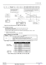
Страница 37: ...nterrupt Block Diagram UIE bit INT output UF bit The time updating Seconds or period period period period 1 0 Hi z L 1 0 Internal operation Write operation tRTN1 tRTN1 tRTN1 7 324 ms to 7 644 ms tRTN1 tRTN1 Figure 28 Time Update Interruption Timing Chart Carry Sec F64Hz Update Control Circuit USEL bit UF 0 Clear Carry Min tRTN1 UF Flag UIE bit INT ...

Страница 38: ...ead 0 POR was not detected 1 POR was detected The result is retained until this bit is cleared to zero The default value of the register is set by power on reset 2 VLF bit VLF are set from POR or XST Table 40 VLF bit Voltage Low Flag VLF Data Description Write 0 Clear for the next detection 1 Ignored Read 0 VLF was not detected 1 POR or XST was detected The result is retained until this bit is cle...

Страница 39: ... 4 bit 3 bit 2 bit 1 bit 0 Bank1 D Extension Register FSEL1 FSEL0 USEL TE WADA TSEL1 TSEL0 14 6 2 FOUT Function Table 1 FSEL1 FSEL0 bit Table 43 FSEL Register Frequency Select FSEL1 FSEL0 TMPIN Output 0 0 x 32768 Hz Output 0 1 0 1024 Hz Output 1 0 1 Hz Output 1 1 x OFF x don t care Timer interrupt output can be assigned to the FOUT pin so when using frequency output set TMPIN 0 and set the timer i...

Страница 40: ... floating When the VLF bit detects 0 1 the default value of backup battery switchover function related registers is set Figure 29 Battery Backup Switchover Function Block Diagram 14 7 2 Related Register of Battery Backup Switchover Function Table 44 Battery backup switchover function related register Address h Function bit 7 bit 6 bit 5 bit 4 bit 3 bit 2 bit 1 bit 0 Bank3 2 Power Switch Control IN...

Страница 41: ... 0 0 OFF OFF Do not select this combination 1 1 OFF OFF Do not select this combination 1 1 1 OFF ON SPI Bus interface ON Other than 1 1 Auto control ON Battery backup switchover function ON When using a non re chargeable battery it is necessary to install a charge protection diode externally Figure 30 Battery backup switchover control Initial power on Voltage detection intermittent timing Table 48...

Страница 42: ...me with setting SW1 VDD VBAT ON OFF intermittently These two bits control SW1 OFF period and user can check much precision voltage by preventing reverse current from VBAT to VDD when main VDD shuts down VDD voltage low detection VDET1 is active anytime so lower voltage detection moves RTC into backup mode immediately regardless SW1 OFF time These SW1 OFF occur every second Refer to Figure 31 Table...

Страница 43: ...14 How to use RX4111CE Jump to Top Bottom ETM62E 02 Seiko Epson Corporation 42 Figure 32 VDD voltage detection SW OFF intermittent operation 2 ms 256 ms ex 256 ms ex 2 ms ...

Страница 44: ...256 s to year Figure 33 Time Stamp function 14 8 2 Related Registers For Time Stamp Functions Table 50 Time Stamp function registers Address h Function bit 7 bit 6 bit 5 bit 4 bit 3 bit 2 bit 1 bit 0 Bank1 D Extension Register FSEL1 FSEL0 USEL TE WADA TSEL1 TSEL0 Bank1 E Flag Register POR UF TF AF EVF VLF XST Bank1 F Control Register z z UIE TIE AIE EIE z STOP Bank2 B Over Write Control No Functio...

Страница 45: ...rrupt Enable Control of INT interrupt output when an event occurs EVF 0 1 Table 52 EIE bit Event Interrupt Enable EIE Data Description Write 0 1 When an event interrupt event occurs an interrupt signal is not generated INT status remains Hi z 2 When an event interrupt event occurs the interrupt signal is canceled INT status changes from low to Hi z 1 When an event interrupt occurs an interrupt sig...

Страница 46: ... of sub seconds from Year without contradiction Table 54 COMTG bit Command Trigger COMTG Data Description Write 0 Time stamp by SPI Bus is disabled 1 Time stamp by SPI Bus available When a reading command to Bank2 address Fh is transmitted by SPI Bus the time is recorded by Bank2 address 0h to 9h The read value of Bank2 address Fh is 0h 2 Time stamp Timing 1 1 1 1 INTpin DI CLK Time stamp trigger ...

Страница 47: ...tamp Record Register Bank2 Address Function Time stamp data 0h Time Stamp 1 1024S 256Hz 512Hz 1h Time Stamp 1 128S 1Hz 256Hz 2h Time Stamp SEC Seconds 3h Time Stamp MIN Minutes 4h Time Stamp HOUR Hours 5h Time Stamp WEEK Day 6h Time Stamp DAY Date 7h Time Stamp MONTH Month 8h Time Stamp YEAR Years 9h Status Stamp RTC Internal status VDET XST Status stamp register Table 56 Status Stamp Address Func...

Страница 48: ...is normal 1 Crystal oscillation stopped or temporarily stopped XST detects more than 10ms stopped The time stamp cannot be recorded at the moment of oscillation stop It is recorded at the moment the oscillation restores 3 EVDET bit Enable VDET Enable Disable control of time stamp VDET Table 60 EDVET bit Enable VDET EVDET Data Description Write 0 No time stamp even VDET is detected 1 Time stamp by ...

Страница 49: ...s 1 1024 seconds and WEEK information are not recorded in the recording area of Bank4 Bank7 1 TSRAM bit Time Stamp RAM Selection of time stamp recording area or USER RAM Table 63 TSRAM bit Time Stamp RAM TSRAM Data Description Write 0 It can read and write as USER RAM Time stamp data is recorded only at addresses Bank2 0h to 8h 1 Bank4 to Bank7 is used as the time stamp recording area To clear the...

Страница 50: ...rom INT Even SPI Bus command trigger is executed it makes no interrupt output 1 TSFUL bit Time Stamp Full 8 time stamp data area full recording Table 66 TSFUL bit TSFUL Data Description Read 0 Time stamp RAM area is not full 1 8 times of time stamp recording area is fully recorded 2 TSEMP bit Time Stamp Empty No recording date in RAM Table 67 Time Stamp Empty bit TSEMP Data Description Read 0 Ther...

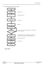
Страница 51: ...individual applications 1 In Initial power on VLF can not be cleared to 0 until internal oscillation starts Start Wait Wait time of 40 ms is necessary at least Whether it is a return from the state of the backup is confirmed VLF 1 YES YES NO VLF 0 clear Wait VLF 0 NO Please set waiting time depending on load of a system optionally It takes about 200 ms from Power ON to oscillation start Power on S...

Страница 52: ...the Alarm registers can be used as a RAM register In such cases be sure to write 0 to the AIE bit Setting the Timer function Set the Wakeup Timer function When the fixed cycle timer function is not being used the Timer Counter register can be used as a RAM register In such cases stop the fixed cycle timer function by writing 0 to the TE and TIE bits When initialization is finished be sure to set S...

Страница 53: ...charge control Write 0C h Adjust the setting of SMPTSEL1 0 when the power switching is difficult with the default values 00b Figure 41 Flow3 3 The setting of the clock and calendar Next process Set time STOP 1 Set STOP bit to 1 to prevent time update in time setting Write current time Write information of year month date day of the week hour minute second which is necessary to set or reset In case...

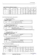
Страница 54: ...ng example of the Wake up timer interrupt function Next process Bank2 1Ah 1Ch Set initial value of down counter Start count Set TE bit to 1 to start timer interrupt function When start timers interrupt function please surely set reset 2 initial value of down counter in advance Fh Set the INT output at event occurrence by setting the TIE bit 1 Countdown is suspended with TSTP 0 1 and countdown is p...

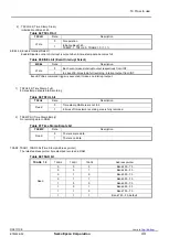
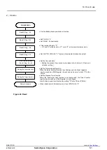
Страница 55: ... Setting example of the Alarm interrupt function Next process Fh Select and set INT output in AIE bit Bank1 Dh Select week or day in WADA bit Eh Clear AF bit Alarm setting Set AIE bit to 0 to stop Alarm interrupt function Set alarm data Bank1 Fh Bank1 7h 9h Bank2 Ch Figure 45 Flow7 ...

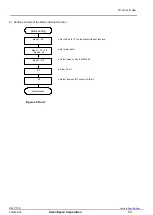
Страница 56: ...n event occurs the EVF bit changes to 1 and an interrupt occurs from the INT pin Bank2 0h 8h Read the time stamp data Start Clear EVF to 0 Set EIE to 1 Bank1 Eh Fh Waiting for event YES NO Clear EIE bit to 0 Bank3 5h Set EVDET or EXST to 1 Bank3 5h Clear EVDET and EXST to 0 to disable the time stamp function Do not generate time stamps while reading time stamp data Bank1 Fh Figure 46 Flow8 ...

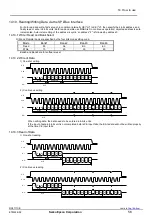
Страница 57: ... 10 2 Write of Data 1 One shot writing CLK C E D I D O Hi Z 0 0 0 1 A3 A2 A1 A0 D7 D6 D5 D4 D3 D2 D1 D0 1 2 3 4 5 6 7 8 9 10 11 12 13 14 15 16 Mode Address N Data N 2 Continuous writing CLK C E D I D O Hi Z 0 0 1 A3 A2 A1 A0 D7 D6 D5 D1 D0 D7 D6 1 2 3 4 5 6 7 8 9 10 11 D1 D0 D7 D6 D1 D0 0 Mode Address N Data N Data N 1 Data N m When writing data the data needs to be entered in 8 bits units If the ...

Страница 58: ...CU connection example VDD RX4111CE MCU VDD VIO VBAT INT IRQ 0 1 μF I V R 1 mA GND GND VDD Primary Battery CR2032 etc Pull Up Resistor Pull up resister 1 kΩ to 5 kΩ is recommended Please confirm DI DO CLK SPI compliant by oscilloscope Please set 0 1 μF bypass capacitor near RTC pin CLK SCLK DI MOSI FOUT SLEEP CLOCK SS DO CE MISO ...

Страница 59: ...terrupt Cycles 30 Table 28 Alarm Interrupt Registers 32 Table 29 WADA bit Week Alarm Day Alarm Select 32 Table 30 AF bit Alarm Flag 33 Table 31 AIE bit Alarm Interrupt Enable 33 Table 32 Alarm Setting Ex1 33 Table 33 Alarm Setting Ex2 33 Table 34 Time Update Interrupt Registers 35 Table 35 USEL bit Update Interrupt Select 35 Table 36 UF bit Update Flag 35 Table 37 UIE bit Update Interrupt Enable 3...

Страница 60: ...re 18 Basic Function 32 768 kHz oscillation counter FOUT 25 Figure 19 Wake up Timer Initial Sequence cycle error 27 Figure 20 Wake up Timer Block Diagram timer source 28 Figure 21 Wake up Timer Start Sequence 30 Figure 22 Wake up Timer Block Diagram 31 Figure 23 Wake up Timer Timing Chart 31 Figure 24 Alarm Interrupt Black Diagram 34 Figure 25 Alarm Interrupt Timing Chart 34 Figure 26 Time Update ...

Страница 61: ...ed Shanghai Branch High Tech Building 900 Yishan Road Shanghai 200233 China Shenzhen Branch Room 603 604 6 Floor Tower 7 One Shenzhen Bay No 3008 Center Rd Shenzhen 518054 China Epson Hong Kong Ltd Unit 715 723 7 F Trade Square 681 Cheung Sha Wan Road Kowloon Hong Kong www epson com hk Epson Taiwan Technology Trading Ltd 15F No 100 Songren Rd Sinyi Dist Taipei City 11073 Taiwan www epson com tw El...

Отзывы: