EPC – EFFICIENT POWER CONVERSION CORPORATION |
WWW.EPC-CO.COM
| COPYRIGHT 2014
EPC Products are distributed
exclusively through Digi-Key.
www.digikey.com
For More Information:
Please contact [email protected]
or your local sales representative
Visit our website:
www.epc-co.com
Sign-up to receive
EPC updates at
bit.ly/EPCupdates
or text “EPC” to 22828
DESCRIPTION
These development boards are in a monolithic half- bridge topology with on-board gate drives,
featuring the EPC2100/1/5 eGaN
IC
s (Enhancement-mode Gallium Nitride Integrated Circuit).
The purpose of these development boards is to simplify the evaluation process of these
monolithically integrated eGaN FETs by including all the critical components on a single board
that can be easily connected into any existing converter.
The development board is 2” x 2” and contains one eGaN
IC
in half-bridge configuration using the
Texas Instruments LM5113 gate driver, supply and bypass capacitors. The board contains all critical
components and layout for optimal switching performance and has additional area to add buck
output filter components on board. There are also various probe points to facilitate simple wave-
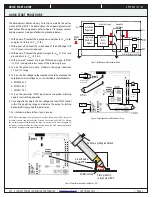
form measurement and efficiency calculation. A complete block diagram of the circuit is given in
Figure 1.
For more information on the EPC2100/1/5 eGaN
IC
s, please refer to the datasheets available from
EPC at www.epc-co.com. The datasheet should be read in conjunction with this quick start guide.
Development Board
EPC9036/37/41
Quick Start Guide
Monolithic Half-Bridge with
Gate Drive for EPC2100/1/5
Demonstration Board Notification
These boards are intended for product evaluation purposes only and are not intended for commercial use. As evaluation tools, they are not designed for compliance with the European Union directive on
electromagnetic compatibility or any other such directives or regulations. As board builds are at times subject to product availability, it is possible that boards may contain components or assembly materials
that are not RoHS compliant. Efficient Power Conversion Corporation (EPC) makes no guarantee that the purchased board is 100% RoHS compliant. No Licenses are implied or granted under any patent
right or other intellectual property whatsoever. EPC assumes no liability for applications assistance, customer product design, software performance, or infringement of patents or any other intellectual
property rights of any kind.
EPC reserves the right at any time, without notice, to change said circuitry and specifications.
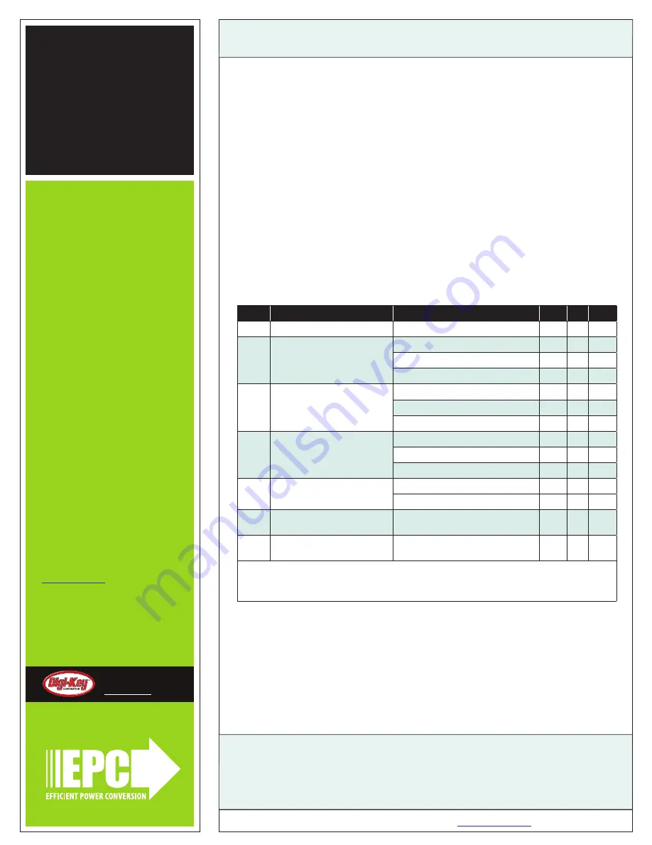
Symbol Parameter
Conditions
Min Max Units
V
DD
Gate Drive Input Supply Range
7
12
V
V
IN
Bus Input Voltage Range
When using 30 V devices, EPC9036
24*
V
When using 60 V devices, EPC9037
48*
V
When using 80 V devices, EPC9041
64*
V
V
OUT
Switch Node Output Voltage
When using 30 V devices, EPC9036
30*
V
When using 60 V devices, EPC9037
60*
V
When using 80 V devices, EPC9041
80*
V
I
OUT
Switch Node Output Current
When using 30 V devices, EPC9036
28*
A
When using 60 V devices, EPC9037
22*
A
When using 80 V devices, EPC9041
20*
A
V
PWM
PWM Logic Input Voltage
Threshold
Input ‘High’
3.5
6
V
Input ‘Low’
0
1.5
V
Minimum ‘High’ State Input
Pulse Width
VPWM rise and fall time < 10ns
50
ns
Minimum ‘Low’ State Input Pulse
Width
VPWM rise and fall time < 10ns
100#
ns
**Maximum input voltage depends on inductive loading, Maximum switch node ringing must be kept under device rated voltage.
* Maximum current depends on die temperature – actual maximum current with be subject to switching frequency, bus voltage and thermal cooling. eGaNIC
intended for high step-down ratio applications.
# Limited by time needed to ‘refresh’ high side bootstrap supply voltage.
Table 1: Performance Summary (T
A
= 25°C)


