


Euro-500TX Handy
© Elcom, s. r. o.
Service manual
10
Euro-500TX Handy
© Elcom, s. r. o.
Service manual
11
2 Circuit schemes and functions
2.1 Power supply circuits
2.1.1 External power supply
The switched pulse power supply circuit ONTOP 100-240 V, 50-60 Hz, 24 V/1.5 A, 36 W serves as the
external power supply for the ECR. Its primary function is to produce unidirectional voltage needed for the
proper ECR functionality from the mains voltage.
2.1.2 Primary power supply
The primary power supply serves as the supply of voltage for the +5 V voltage source in the case that the
external power supply is connected. This circuit is built around the MC34063 universal unidirectional vol-
tage changer that guarantees high resistance to the mains interference. Its high efficiency (80 %) secures
effective voltage conversion and low heat emissions (low cooling demands). The output voltage is approx.
8.25 V and is marked as VSS in the scheme.
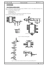
2.1.3 The +5 V power source (VCC) and the NMI signal generator
This power source manufactures the VRAM and VCC voltages. VCC voltage is needed for the circuits that
are at all times powered as the ECR is on. The KA278R05 linear voltage stabiliser is at the heart of this
circuit that fixedly su5 V voltage. Figure 2.2 shows the NMI signal generator as well and this circuit
features NCP301 comparator with threshold level 4.5 V. The main use for the NMI signal is that informs
the microprocessor of the voltage drop and is also used to shut down all the power sources. The D4 diode
produces the VRAM voltage, the R9 resistor ensures the constant charging of the BT1 NiCd accumulator
while the ECR is on, and the JP1 jumper is used for ECR clearing. The figure also shows the PWRSW that
is used to connect the main ECR power switch.
C1
1u/35V
C2
1u/35V
3
4
2
1
EMI
FILTER
.
.
EF1
2x3,3mH/1,5A
VIN
ADP+
ADP-
D1
MBRS340T3
8
7
6
5
1
2
3
4
U13
MC34063
R20
0R22
R21
1k
R22
5k6
C4
470p
L1
120uH
D3
FMKA140
C5
330u/25V
VSS
C3
330u/25V
F2
1.85A
VINf
Fig. 2.1 Primary power supply
R5
150k
R9
1k0/F
C9
2200u/25V
BT1
3V6, 60mAh
VCC
VRAM
D4
FMKA140
2
1
4
3
U14
KA278R05
JP1
Batt 3p
NMI
1
2
PWRSW
AVA 5400-2P-S
C13
100n
C70
100n
R30
0R
NMI
VBAT1
R6
22k
R
S
T
1
IN
2
G
N
D
3
4
N
.C
.
N
.C
.
5
U12
NCP301LSN45T1
D15
FMKA140
VSS
Fig. 2.2 +5 V power supply and the NMI signal generator