background image


Prometheus CPU User Manual V1.44 

Page 63 

22. FLASHDISK  MODULE 

Prometheus is designed to accommodate an optional flashdisk module. This module contains 
32MB to 128MB of solid state non-volatile memory that operates like an IDE drive without 
requiring any additional driver software support. 


Model Capacity 

FD-32

 32MB 

FD-64

 64MB 

FD-96

 96MB 

FD-128

 128MB 


22.1 Installing the Flashdisk Module 

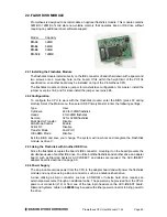
The flashdisk module installs directly on the IDE connector J8 and is held down with a spacer and 
two screws onto a mounting hole on the board. It fits within the height limit of the PC/104 
specification, so another board may be installed on top of the Prometheus CPU. 

The flashdisk module contains a jumper for master/slave configuration. For master, install the 
jumper over pins 1&2, and for slave install the jumper over pins 2&3. 

22.2 Configuration 

To configure the CPU to work with the Flashdisk module, enter the BIOS (press F2 during 
startup). Select the Main menu, then select IDE Primary Master. Enter the following settings: 

Type: User 
Cylinders: 

489 for 32MB flashdisk 

Heads: 

4 for 32MB flashdisk 

Sectors: 

32 for 32MB flashdisk 

Multi Sector Transfer: 

Disable 

LBA Mode Control: 

Enable 

32 Bit I/O: 

Disable 

Transfer Mode: 

Fast PIO 1 

Ultra DMA Mode: 

Disable 

Exit the BIOS and save your change. The system will now boot and recognize the FlashDisk 
module as drive C:. 

22.3 Using the Flashdisk with Another IDE Drive 

Since the flashdisk occupies the board’s IDE connector, mounting it on the board prevents the 
simultaneous use of another IDE drive. To utilize both the flashdisk and another drive, an adapter 
board, such as Diamond Systems’ ACC-IDEEXT, and cables are required. The ACC-IDEEXT 
adapter board is described on page 69. 

22.4 Power Supply 

The 44-pin cable carries power from the CPU to the adapter board and will power the flashdisk 
module and any drive using a 44-pin connector, such as a notebook hard drive.  

A drive utilizing a 40-pin connector, such as a CD-ROM or full-size hard drive, requires an 
external power source through an additional cable. The power may be provided from the CPU’s 
power out connector (J12) or from one of the two 4-pin headers on the ACC-IDEEXT board. 
Diamond Systems’ cable no. 

698006

 may be used with either power connector to bring power to 

the drive. 

Содержание PROMETHEUS PR-Z32-E-ST

Страница 1: ...ration PC 104 CPU with Ethernet and Data Acquisition Models PR Z32 E ST PR Z32 EA ST User Manual V1 44 Copyright 2003 Diamond Systems Corporation 8430 D Central Ave Newark CA 94560 Tel 510 456 7800 ww...

Страница 2: ...NOTES ON OPERATING SYSTEMS AND BOOTING PROCEDURES 28 9 1 BOOTING TO DOS FROM A FLOPPY DRIVE 28 9 2 INSTALLING AN OS FROM A FLOPPY DRIVE ONTO A FLASHDISK MODULE 28 10 DATA ACQUISITION CIRCUIT 30 11 DA...

Страница 3: ...ITION SPECIFICATIONS 62 22 FLASHDISK MODULE 63 22 2 CONFIGURATION 63 22 3 USING THE FLASHDISK WITH ANOTHER IDE DRIVE 63 22 4 POWER SUPPLY 63 23 I O PANEL BOARD 64 24 FLASH DISK PROGRAMMER BOARD 69 25...

Страница 4: ...mounting holes in each corner The result is an extremely rugged computer system fit for mobile and miniature applications PC 104 modules stack together with 0 6 spacing between boards 0 662 pitch inc...

Страница 5: ...pin version for notebook drives Accepts solid state flashdisk modules directly on board 100BaseT full duplex PCI bus mastering Ethernet 100Mbps IrDA port requires external transceiver PS 2 keyboard a...

Страница 6: ...xternal A D triggering 48 sample FIFO for reliable high speed sampling and scan operation Analog Output 4 analog outputs 12 bit resolution 10V and 0 10V output ranges Simultaneous update Adjustable ou...

Страница 7: ...J4 Ethernet port J5 Dual USB ports J7 Floppy drive connector J8 IDE drive connector J11 Input power connector J12 Switched output power connector J14 Data acquisition I O connector J15 Auxiliary seria...

Страница 8: ...ral latches for enhanced reliability Each ribbon cable has 40 wires Cable A Cable B 1 DCD1 1 STB 2 DSR 1 2 AFD 3 RXD 1 3 PD0 4 RTS 1 4 ERR COM 1 5 TXD 1 5 PD1 6 CTS 1 6 INIT 7 DTR 1 7 PD2 8 RI 1 8 SLI...

Страница 9: ...Out The signal on this pin is referenced to 5V Out Connect a speaker between this pin and 5V Out IDE Drive LED Referenced to 5V Out Does not require a series resistor Connect LED directly between this...

Страница 10: ...upply voltage level Many boot up problems are caused simply by insufficient voltage due to excess current draw on the 5V supply Multiple 5V and Ground pins are provided for extra current carrying capa...

Страница 11: ...d full size power connector for a hard drive or CD ROM drive and a standard miniature power connector for a floppy drive 4 4 Ethernet J4 1 Common 2 RX 3 Common 4 RX 5 TX 6 TX J4 is a 1x6 pin header It...

Страница 12: ...e Features J6 ZFIX 1 2 Ground 3 3V 3 4 WDI PRST 5 6 WDO J6 serves two main functions It is used for watchdog timer access and it is used to enable the ZFx86 failsafe feature ZFIX mode for reprogrammin...

Страница 13: ...ector at the far end of the cable after the twist is for Drive A and the middle connector is for Drive B 4 9 IDE Drive J8 RESET 1 2 Ground D7 3 4 D8 D6 5 6 D9 D5 7 8 D10 D4 9 10 D11 D3 11 12 D12 D2 13...

Страница 14: ...34 Aground Vin Vin 0 35 36 Vin 8 Vin 1 37 38 Vin 9 Vin 2 39 40 Vin 10 Vin 3 41 42 Vin 11 Vin 4 43 44 Vin 12 Vin 5 45 46 Vin 13 Vin 6 47 48 Vin 14 Vin 7 49 50 Vin 15 Signal Name Definition DIO A7 A0 Di...

Страница 15: ...104 connectors are along the bottom edge of the board View from Top of Board J2 PC 104 16 bit bus connector J1 PC 104 8 bit bus connector Ground D0 C0 Ground IOCHCHK A1 B1 Ground MEMCS16 D1 C1 SBHE S...

Страница 16: ...ate setting will work properly and provide faster performance However it should be tested in your application to verify correct operation In standard configuration the CPU issues 2 wait states for 16...

Страница 17: ...he default setting 5 2 J6 Watchdog Timer System Recovery J6 is used to configure the watchdog timer and enable system recovery failsafe mode in case of BIOS corruption This jumper has different dimens...

Страница 18: ...chip selects and 4 user configurable memory chip selects These chip selects are visible in the BIOS setup screens Three of the I O chip selects are used by the Prometheus design Chip selects 1 and 2 a...

Страница 19: ...boots console redirection is disabled There are three possible configurations for console redirection POST only default Always On Disabled To modify the console redirection settings enter the BIOS se...

Страница 20: ...triggered it begins to count down When it reaches zero it triggers WD2 and may also generate a user selectable combination of these events Non maskable interrupt NMI System controller interrupt SCI S...

Страница 21: ...oot ROM and provide user I O through COM1 At this point the DSC utility program ZFTERM EXE may be used to download the BIOS to the board See the information in the Utilities BIOS Recovery folder of th...

Страница 22: ...as serial ports COM1 and COM2 I O Device Configuration Data Acquisition The on board data acquisition circuit is modified on the same screen as serial ports COM3 and COM4 ISA I O Chip Select Setup Flo...

Страница 23: ...When the Prometheus CPU boots up you will see the BUR display in the terminal program The required communication parameters are 9600 n 8 1 Now run the accompanying batch file recover bat to begin the...

Страница 24: ...ecovery section of the users manual or the instructions included with the BIOS upgrade package on our website Boot the system and enter the BIOS setup by pressing F2 early in the boot up Go to Advance...

Страница 25: ...form of wear leveling Each time data is written the next consecutive available memory space is used and the current location is marked as garbage and made available for later use This way the system...

Страница 26: ...It is connected to the ZfX86 CPU via the board s internal PCI bus It resides at address 1000 and uses IRQ 10 The Prometheus Software CD includes Ethernet drivers for Windows 95 Windows 98 Windows NT...

Страница 27: ...ected on the Advanced menu of the BIOS Select Advanced Chipset Control then ISA I O Chip Select Setup I O Window io_cs1 is for COM3 and I O window io_cs2 is for COM4 The only parameter that may be cha...

Страница 28: ...OM4 and the Data Acquisition System 5 Save the new settings and exit the BIOS 6 The system will now boot to DOS from the floppy drive 9 2 Installing an OS From a Floppy Drive onto a Flashdisk Module 1...

Страница 29: ...ower cable is required The power may be provided either from one of the two 4 pin headers on the extender board or from the Auxiliary Power Out connector J12 on the Prometheus CPU Use DSC cable no 698...

Страница 30: ...ng is supported with interrupts and a FIFO The FIFO is used to store a user selected number of samples and the interrupt occurs when the FIFO reaches this threshold Once the interrupt occurs an interr...

Страница 31: ...fault 280h Read Write control Read Write Window data width 8 bits Active Level Active Low Window size 16 A functional list of registers is provided below and detailed bit definitions are provided on t...

Страница 32: ...0 CTRD9 CTRD8 14 CTRD23 CTRD22 CTRD21 CTRD20 CTRD19 CTRD18 CTRD17 CTRD16 15 CTRNO LATCH GTDIS GTEN CTDIS CTEN LOAD CLR READ Blank bits are unused and read back as 0 Address 7 6 5 4 3 2 1 0 0 AD7 AD6 A...

Страница 33: ...elected by ADCLK in base 4 bit 5 RSTBRD Reset the entire board excluding the D A Writing a 1 to this bit causes all registers on the board to be reset to 0 The effect on the digital I O is that all po...

Страница 34: ...g from 32768 to 32767 This raw A D value must then be converted to the corresponding input voltage and or the engineering units represented by that voltage by applying additional application specific...

Страница 35: ...settling During this time an A D conversion should not be performed because the data will be inaccurate After writing a new gain setting Base 3 the WAIT bit is also set and the program must monitor i...

Страница 36: ...input pin The gain setting is the same for all input channels When this register is written to the WAIT bit Read Base 3 bit 6 will go high for 10 microseconds to indicate that the analog input circui...

Страница 37: ...gh for 9 microseconds The program should monitor this bit after writing to either register and wait for it to become 0 prior to starting an A D conversion DACBSY Indicates the DAC is busy updating app...

Страница 38: ...upts will be on the same interrupt level The user s interrupt routine must monitor the status bits to know which circuit has requested service After processing the data but before exiting the interrup...

Страница 39: ...DA0 is the LSB D A data is an unsigned 12 bit value This register must be written to before Base 7 since writing to Base 7 updates the DAC immediately Base 6 Read A D Channel and FIFO Status Bit No 7...

Страница 40: ...ue Base 7 Read Analog Operation Status Bit No 7 6 5 4 3 2 1 0 Name DMAINT TINT DINT AINT ADCH3 ADCH2 ADCH1 ADCH0 DMAINT DMA interrupt status 1 interrupt pending 0 interrupt not pending TINT Timer inte...

Страница 41: ...6 5 4 3 2 1 0 Name DIOCTR X X DIRA DIRCH X DIRB DIRCL The bit assignments of this register are designed to be compatible with the 82C55 chip s control register DIOCTR Selects counter I O signals or d...

Страница 42: ...nternal load register is loaded Upon issuing a Load command through Base 15 the selected counter s associated register will be loaded with this value For counter 0 it is the middle byte For counter 1...

Страница 43: ...TEn signal is low counting is disabled CTDIS Disable counting on the selected counter The counter will ignore input pulses CTEN Enable counting on the selected counter The counter will decrement on ea...

Страница 44: ...ster is used to control the counter timers A counter is selected with bit 7 and then a 1 is written to any ONE of bits 6 0 to select the desired operation for that counter The other bits and associate...

Страница 45: ...is oriented vertically The functions are shown below and are described in detail on the following page The default settings are as shown The various configurations are illustrated and described below...

Страница 46: ...on Prometheus without damage is 35V If you connect the analog inputs on Prometheus to a circuit whose ground potential plus maximum signal voltage exceeds 35V the analog input circuit may be damaged C...

Страница 47: ...onfiguration is done with a jumper and applies to all inputs In addition you can select a gain setting for the inputs which causes them to be amplified before they reach the A D converter The gain set...

Страница 48: ...oup of consecutively numbered channels you do not need to write the input channel prior to each conversion For example to read from channels 0 2 write Hex 20 to base 2 The first conversion is on chann...

Страница 49: ...se a loop with a timeout int checkstatus returns 0 if ok 1 if error int i for i 0 i 10000 i if inp base 3 0x80 then return 0 conversion completed return 1 conversion didn t complete 14 6 Read the data...

Страница 50: ...ue 32768 Full scale input range Example Input range is 5V and A D value is 17761 Input voltage 17761 32768 5V 2 710V For a bipolar input range 1 LSB 1 32768 Full scale voltage Here is an illustration...

Страница 51: ...e set to a number at least equal to the scan size and in all cases equal to an integral number of scans For example if the scan size is 8 channels the FIFO threshold should be set to 8 16 24 32 40 or...

Страница 52: ...ls between LOW and HIGH will be sampled STS stays high during the entire scan multiple A D conversions No interrupt occurs The user program monitors STS and reads all A D values when it goes low 1 0 S...

Страница 53: ...esolution The resolution is the smallest possible change in output voltage For a 12 bit DAC the resolution is 1 212 or 1 4096 of the full scale output range This smallest change results from an increa...

Страница 54: ...de 0 10V Full scale range 10V 0V 10V Desired output voltage 2 000V D A code 2 000V 10V 4096 819 2 819 Note the output code is always an integer For the unipolar output range 0 10V 1 LSB 1 4096 10V 2 4...

Страница 55: ...0V 10V 20V Desired output voltage 2 000V D A code 2V 10V 2048 2048 2457 6 2458 For the bipolar output range 10V 1 LSB 1 4096 20V or 4 88mV Here is an illustration of the relationship between D A code...

Страница 56: ...LSB and MSB values LSB D A Code 255 keep only the low 8 bits MSB int D A code 256 strip off low 8 bits keep 4 high bits Example Output code 1776 LSB 1776 255 240 F0 Hex MSB int 1776 256 int 6 9375 6 T...

Страница 57: ...nt Configure the circuit for Unipolar A D mode The gain setting and single ended vs differential mode do not matter Input 0V to any input channel and perform A D conversions on that channel Adjust R67...

Страница 58: ...O header J14 see page 14 They are 3 3V and 5V logic compatible Each output is capable of supplying 8mA in logic 1 state and 12mA in logic 0 state See the specifications on page 62 for more detail DIR...

Страница 59: ...nter value can be latched for reading 20 2 Counter 1 Counting Totalizing Functions The second counter Counter 1 is similar to Counter 0 except it is a 16 bit counter It also has an input a gate and an...

Страница 60: ...If disabled the counter will ignore incoming clock edges The gating may be enabled or disabled at any time When gating is disabled the counter will count all incoming edges When gating is enabled if t...

Страница 61: ...15 0x10 outp base 15 0x90 The counter will run only when the gate input is high Disabling the counter gate Counter 0 Counter 1 outp base 15 0x20 outp base 15 0xA0 The counter will run continuously Cl...

Страница 62: ...A resolution 12 bits 1 4096 of full scale Output ranges Unipolar 0 10V or user programmable Bipolar 10V or user programmable Output current 5mA max per channel Settling time 4 S max to 1 2 LSB Relativ...

Страница 63: ...ders 489 for 32MB flashdisk Heads 4 for 32MB flashdisk Sectors 32 for 32MB flashdisk Multi Sector Transfer Disable LBA Mode Control Enable 32 Bit I O Disable Transfer Mode Fast PIO 1 Ultra DMA Mode Di...

Страница 64: ...ting in increased ruggedness and quicker assembly In addition a standard precut cover plate is available to enable mounting the panel board and CPU in Diamond Systems Pandora enclosure system The pane...

Страница 65: ...h as a video board or DC DC power supply Location Type Description J3 Pin header Speaker and miscellaneous functions J5 Pin header Power connection to DC DC power supply input J12 Pin header Power con...

Страница 66: ...V 5V 12V and or 12V these voltages can be supplied through J13 as well The 5V and 12V are controlled by the CPU s ATX power circuit while the 5V and 12V are connected directly to the PC 104 bus pins J...

Страница 67: ...when the two wires are on the two end positions of the housing External momentary switches may be connected to J3 to control power or reset For power connect the switch between pins 1 and 2 of J3 For...

Страница 68: ...to the connectors of the CPU board being careful to align all the connectors properly Note that there are mating connectors on all 4 edges of the board for the EA analog I O version and connectors on...

Страница 69: ...are provided for the external hard drive or CD ROM drive A dedicated connector J2 is provided for the flashdisk module Any two devices may be connected simultaneously using this board with proper mast...

Страница 70: ...ial ports 1 or 2 the serial port signals must terminate to another board or interference problems may occur that will slow down the performance of your CPU Photo No Cable No Description 2 C PRZ 01 80...

Страница 71: ...013 The pinout of this cable is shown below Each row represents one wire on the cable PL5 pin no PL5 Signal J25 pin no J25 Signal 1 Red 1 Red 2 Red Return 2 Ground 3 Green 3 Green 4 Not connected 4 Gr...

Страница 72: ...the vertical I O headers on the board If you need to use IDE floppy or switched power output you will need to use cables to access the corresponding I O headers The following is a list of I O headers...

Страница 73: ...Prometheus CPU User Manual V1 44 Page 73...

Страница 74: ...User Manual V1 44 Page 74 28 PC 104 MECHANICAL DRAWING The following drawing is from the PC 104 specification This document may be downloaded from www pc104 org or from www diamondsystems com support...

Отзывы: