background image


Elektra CPU User Manual V1.00 

Page 8 


Digital I/O 

  24 programmable digital I/O, 3.3V and 5V logic compatible 

  Input voltage Logic 0: -0.5V min, 0.8V max 

  Logic 1: 2.0V min, 5.5V max  

  Input current ±3µA max  

  Output voltage Logic 0: 0.0V min, 0.4V max 

  Logic 1: 2.4V min, 3.3V max  

  Output current Logic 0: 12mA max  

  Logic 1: -8mA max  

  I/O capacitance 20pF max 

  ESD protection: 2KV, contact human body model 

Counter/Timers 

  1 24-bit counter/timer for A/D sampling rate control 

  1 16-bit counter/timer for user counting and timing functions 

  Programmable gate and count enable 

  Internal and external clocking capability 


Содержание ELEKTRA FD-128

Страница 1: ...h Integration CPU with Ethernet and Data Acquisition User Manual Revision 1 01 Document 7650530 Copyright 2005 Diamond Systems Corporation 8430 D Central Ave Newark CA 94560 Tel 510 456 7800 www diamo...

Страница 2: ...rt 26 6 4 Flash Memory 27 6 5 Backup Battery 27 6 6 System Reset 27 7 BIOS 28 7 1 BIOS Settings 28 7 2 BIOS Console Redirection Settings 30 8 SYSTEM I O 31 8 1 Ethernet 31 8 2 Serial Ports 31 8 3 PS 2...

Страница 3: ...ale Error Bookmark not defined 17 ANALOG CIRCUIT CALIBRATION RESOURCES 67 17 1 Analog Circuit Calibration Procedures 68 17 2 Using EEPROM 69 17 2 1 Reading Value from EEPROM 69 17 2 2 Writing value to...

Страница 4: ...or 19 Table 12 System Resources 24 Table 13 I O COM3 4 Control Register Definition 25 Table 14 J11 Ethernet Connector 31 Table 15 COM PORT Default Resource Listing 31 Table 16 Data Acquisition Analog...

Страница 5: ...ection system in place of card edge connectors as well as mounting holes in each corner The result is an extremely rugged computer system fit for mobile and miniature applications PC 104 modules stack...

Страница 6: ...USB 1 1 ports IDE drive connectors 44 pin notebook drive connection Accepts solid state flash disk module directly on board 10 100 BaseT full duplex PCI bus mastering Ethernet 100Mbps or 10Mbps Infra...

Страница 7: ...ime to 0 012 10uS Channel to channel matching 1LSB Fullscale accuracy of 1LSB when using auto calibration Not more than 10ppm oC worse case drift accuracy when using auto calibration over the specifie...

Страница 8: ...x Output voltage Logic 0 0 0V min 0 4V max Logic 1 2 4V min 3 3V max Output current Logic 0 12mA max Logic 1 8mA max I O capacitance 20pF max ESD protection 2KV contact human body model Counter Timers...

Страница 9: ...ts J6 Watchdog Failsafe Features J8 IDE drive connector J9 External battery connector J10 Jumper Block J11 Input power connector J12 Switched output power connector J14 Data acquisition I O connector...

Страница 10: ...104 connector and the board is oriented so that the PC 104 connectors are along the bottom edge of the board View from Top of Board J2 PC 104 16 bit bus connector J1 PC 104 8 bit bus connector Ground...

Страница 11: ...DSR 1 2 AFD 3 RXD 1 3 PD0 4 RTS 1 4 ERR COM 1 5 TXD 1 5 PD1 6 CTS 1 6 INIT 7 DTR 1 7 PD2 8 RI 1 8 SLIN 9 Ground 9 PD3 10 DCD 2 10 Ground 11 DSR 2 11 PD4 12 RXD 2 12 Ground 13 RTS 2 LPT 1 13 PD5 COM 2...

Страница 12: ...Out The signal on this pin is referenced to 5V Out Connect a speaker between this pin and 5V Out Speaker support not mentioned in pc speaker IDE Drive LED Referenced to 5V Out Does not require a seri...

Страница 13: ...Elektra CPU User Manual V1 00 Page 13 Board mount socket 3M Robinson Nugent no P50 080S R1 TG DSC no 580884...

Страница 14: ...ingle wire each In this case the first 4 pins may be connected to a standard 4 pin miniature PC power connector if desired For a larger PC 104 stack the total power requirements should be calculated t...

Страница 15: ...ovides a standard full size power connector for a hard drive or CD ROM drive and a standard miniature power connector for a floppy drive Connector Part Numbers J12 Connector on CPU board Digi Key Corp...

Страница 16: ...Elektra CPU User Manual V1 00 Page 16 J5 Connector on CPU board Standard 2x5 0 1 header with pin 1 removed J5 Mating Cable Connector Oupiin 4072 2X5H Standard PC USB Header Interface...

Страница 17: ...Used DRQ 21 22 Ground IDEIOW 23 24 Ground IDEIOR 25 26 Ground IORDY 27 28 Ground DACK 29 30 Ground IRQ14 31 32 Pulled low for 16 bit operation A1 33 34 Not Used A0 35 36 A2 CS0 37 38 CS1 LED 39 40 Gr...

Страница 18: ...in 8 Vin 1 37 38 Vin 9 Vin 2 39 40 Vin 10 Vin 3 41 42 Vin 11 Vin 4 43 44 Vin 12 Vin 5 45 46 Vin 13 Vin 6 47 48 Vin 14 Vin 7 49 50 Vin 15 Table 9 J14 Data Acquisition Connector Pin out Signal Name Defi...

Страница 19: ...header is provided for auxiliary access to serial ports 1 and 2 with signals RX TX and Ground for each port This connector may be used in low cost limited I O configurations as an alternative to the...

Страница 20: ...hared IRQ at one time True IRQ sharing where all 3 devices can run simultaneously is not supported here except with software driver check To support true IRQ sharing for all 3 devices for every IRQ ca...

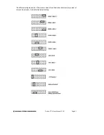
Страница 21: ...Elektra CPU User Manual V1 00 Page 21 The different configurations for J10 are shown below Each illustration shows only the jumper of interest An asterisk indicates the default setting...

Страница 22: ...on the following page AS A D Single ended Differential AU A D Unipolar Bipolar DU D A Unipolar Bipolar The default settings are as shown The various configurations are illustrated and described below...

Страница 23: ...g input circuit may be damaged Check the ground difference between the input source and ELEKTRA before connecting analog input signals NOTE In enhanced mode single ended differential can be overwritte...

Страница 24: ...O 1F0 1F7 14 A D Circuit when applicable I O 280 28F 5 Watchdog Timer Serial Port FPGA Enable Disable I O 25C 25F Ethernet BIOS OS dependant BIOS OS dependant USB BIOS OS dependant BIOS OS dependant T...

Страница 25: ...I O COM3 4 Control Register Definition 0x25F Write Chip select enable disable Bit No 7 6 5 4 3 2 1 0 Name COM4EN COM3EN FPGAEN WDEN COM4EN COM4 chip select enable 1 enable COM4 CS 0 disable COM4 CS C...

Страница 26: ...urations trap special characters The default ELEKTRA BIOS setting disables console redirection after BIOS Power on Self Test POST There are three possible configurations for console redirection POST o...

Страница 27: ...ck backup A connector and jumper are provided to disable the on board battery and enable use of an external battery instead With a battery current of no more than 3uA the on board battery life shall b...

Страница 28: ...rmance These cache settings can make a huge difference for low level BIOS calls and as such can severely limit performance if they are disabled The Frame Buffer size can be increased for specific appl...

Страница 29: ...the OS power management settings will pre empt these settings The only power management mode supported by the system is Power On Suspend other suspend modes are not supported and should not be used u...

Страница 30: ...to COM 2 will be enabled regardless of the COM PORT settings elsewhere Continue CR After POST Off default or On o Determines whether the system is to Wait for CR over COM PORT before continuing after...

Страница 31: ...for testing the chip and accessing the configuration EEPROM Each board is factory configured for a unique MAC address using this program To run the program you must boot the computer to DOS The progra...

Страница 32: ...dedicated for mouse function The two PS 2 ports are accessible via a cable assembly DSC C PRZ 01 attached to J3 Support for these ports is independent of and in addition to mouse and keyboard support...

Страница 33: ...Follow the instructions for installing Windows 9 1 1 DRIVER INSTALLATION 4 Install the National Semiconductors Network driver 5 The USB driver for the floppy drive needs to be loaded before the USB fl...

Страница 34: ...uence below 1 Enable the following in BIOS a Legacy USB support 2 Change BIOS boot sequence so system boots through USB floppy drive 3 Insert DOS installation floppy disk into USB floppy drive and sta...

Страница 35: ...A D sampling rates and a 16 bit counter timer for user applications High speed A D sampling is supported with interrupts and a FIFO The FIFO is used to store a user selected number of samples and the...

Страница 36: ...wing chapter Base Write Function Read Function 0 Command register A D LSB 1 Not used A D MSB 2 A D channel register A D channel register 3 A D gain and scan settings A D gain and status read back 4 In...

Страница 37: ...RD11 CTRD10 CTRD9 CTRD8 14 CTRD23 CTRD22 CTRD21 CTRD20 CTRD19 CTRD18 CTRD17 CTRD16 15 CTRNO LATCH GTDIS GTEN CTDIS CTEN LOAD CLR READ Blank bits are unused and read back as 0 Address 7 6 5 4 3 2 1 0 0...

Страница 38: ...er Page 1 READ Blank bits are unused and read back as 0 Address 7 6 5 4 3 2 1 0 12 D7 D6 D5 D4 D3 D2 D1 D0 13 A7 A6 A5 A4 A3 A2 A1 A0 14 TDBUSY EEBUSY CMUXEN TDACEN 15 FPGA Revision Code Page 2 WRITE...

Страница 39: ...l selected by ADCLK in base 4 bit 5 RSTBRD Reset the entire board excluding the D A Writing a 1 to this bit causes all registers on the board to be reset to 0 The effect on the digital I O is that all...

Страница 40: ...t No 7 6 5 4 3 2 1 0 Name 1 0 1 0 0 1 1 0 1 0 Writing 0xA5 to this register enables the enhanced features of the register map Writing 0xA6 to this register disables the enhanced features of the regist...

Страница 41: ...ettling During this time an A D conversion should not be performed because the data will be inaccurate After writing a new gain setting Base 3 the WAIT bit is also set and the program must monitor it...

Страница 42: ...re only active if enhanced features are enabled otherwise the page is stuck at 0 The page bits control register map addresses 12 through 15 The page bits cannot be read back When this register is writ...

Страница 43: ...for 9 microseconds The program should monitor this bit after writing to either register and wait for it to become 0 prior to starting an A D conversion DACBSY Indicates the DAC is busy updating appro...

Страница 44: ...upts will be on the same interrupt level The user s interrupt routine must monitor the status bits to know which circuit has requested service After processing the data but before exiting the interrup...

Страница 45: ...Current FIFO depth This value indicates the number of A D values currently stored in the FIFO Base 6 B Read A D Channel and FIFO Status Bit No 7 6 5 4 3 2 1 0 Name 0 0 0 0 OVF FF HF EF They are enable...

Страница 46: ...User Manual V1 00 Page 46 OVF Overflow flag Chapter 2 FIFO has overflowed data has been lost This flag is cleared on the next successful A D read 0 FIFO has not overflowed since the last time A D dat...

Страница 47: ...Base 7 Read Analog Operation Status Bit No 7 6 5 4 3 2 1 0 Name DMAINT TINT DINT AINT ADCH3 ADCH2 ADCH1 ADCH0 DMAINT DMA interrupt status 1 interrupt pending 0 interrupt not pending TINT Timer interr...

Страница 48: ...5 4 3 2 1 0 Name DIOCTR X X DIRA DIRCH X DIRB DIRCL The bit assignments of this register are designed to be compatible with the 82C55 chip s control register DIOCTR Selects counter I O signals or dig...

Страница 49: ...this register an internal load register is loaded Upon issuing a Load command through Base 15 the selected counter s associated register will be loaded with this value For counter 0 it is the middle...

Страница 50: ...GATEn signal is low counting is disabled CTDIS Disable counting on the selected counter The counter will ignore input pulses CTEN Enable counting on the selected counter The counter will decrement on...

Страница 51: ...gister is used to control the counter timers A counter is selected with bit 7 and then a 1 is written to any ONE of bits 6 0 to select the desired operation for that counter The other bits and associa...

Страница 52: ...o this register will be written to the selected device During EEPROM read operations this register contains the data to be read from the EEPROM and is valid after EEBUSY 0 The TrimDAC data cannot be r...

Страница 53: ...auses the board to reload the calibration settings from EEPROM CMUXEN Calibration multiplexor enable The cal mux is used to read precision on board reference voltages that are used in the auto calibra...

Страница 54: ...xA5 binary 10100101 to this register each time after setting the PAGE bit in order to get access to the EEPROM This helps prevent accidental corruption of the EEPROM contents Page 1 Base 15 Read FPGA...

Страница 55: ...also set to this value when enhanced features are disabled In this mode the FIFO interface acts identically to the Prometheus Even though the ELEKTRA is using an external FIFO the FPGA must track the...

Страница 56: ...reads back as the last value written to SDOUT If SDOEN 0 this bit reads back as the logical state of the input to this pin at J13 ADUOEN ADUNIP output enable If this bit is enabled the register settin...

Страница 57: ...ith a jumper and applies to all inputs In addition you can select a gain setting for the inputs which causes them to be amplified before they reach the A D converter The gain setting is controlled in...

Страница 58: ...p of consecutively numbered channels you do not need to write the input channel prior to each conversion For example to read from channels 0 2 write Hex 20 to base 2 The first conversion is on channel...

Страница 59: ...a loop with a timeout int checkstatus returns 0 if ok 1 if error int i for i 0 i 10000 i if inp base 3 0x80 then return 0 conversion completed return 1 conversion didn t complete 12 6 Read the data f...

Страница 60: ...32768 Full scale input range Example Input range is 5V and A D value is 17761 Input voltage 17761 32768 5V 2 710V For a bipolar input range 1 LSB 1 32768 Full scale voltage Here is an illustration of...

Страница 61: ...f the scan size is 8 channels the FIFO threshold should be set to 8 16 24 32 40 48 or in expanded FIFO mode 256 but not less than 8 This way the interrupt will occur at the end of the scan and the int...

Страница 62: ...and HIGH will be sampled STS stays high during the entire scan multiple A D conversions No interrupt occurs The user program monitors STS and reads all A D values when it goes low 1 0 Single A D conve...

Страница 63: ...lution The resolution is the smallest possible change in output voltage For a 12 bit DAC the resolution is 1 212 or 1 4096 of the full scale output range This smallest change results from an increase...

Страница 64: ...0 10V Full scale range 10V 0V 10V Desired output voltage 2 000V D A code 2 000V 10V 4096 819 2 819 Note the output code is always an integer For the unipolar output range 0 10V 1 LSB 1 4096 10V 2 44m...

Страница 65: ...10V 20V Desired output voltage 2 000V D A code 2V 10V 2048 2048 2457 6 2458 For the bipolar output range 10V 1 LSB 1 4096 20V or 4 88mV Here is an illustration of the relationship between D A code an...

Страница 66: ...B and MSB values LSB D A Code 255 keep only the low 8 bits MSB int D A code 256 strip off low 8 bits keep 4 high bits Example Output code 1776 LSB 1776 255 240 F0 Hex MSB int 1776 256 int 6 9375 6 The...

Страница 67: ...3 TrimDAC Enable when 1 note that this is mutually exclusive with EE_EN control Table 18 Calibration Control Signal Listing AUTO CALIBRATION TABLE When Register bit CMUXEN 1 the board is in auto calib...

Страница 68: ...full effect in all modes 16 1 Analog Circuit Calibration Procedures Calibration applies only to boards with the analog I O circuitry The analog I O circuit is calibrated during production test prior...

Страница 69: ...base 15 0xA5 unlock EEPROM outp base 13 0x80 set address location to 128 0x80 outp base 14 0xC0 Initiate transfer set to read while inp base 14 0x20 Wait for EEPROM load to complete Data inpb base 12...

Страница 70: ...header J14 see page 18 They are 3 3V and 5V logic compatible Each output is capable of supplying 8mA in logic 1 state and 12mA in logic 0 state See the specifications on page 78 for more detail DIRA D...

Страница 71: ...unting Totalizing Functions The second counter Counter 1 is similar to Counter 0 except it is a 16 bit counter It also has an input a gate and an output These signals may be user provided on the I O h...

Страница 72: ...disabled the counter will ignore incoming clock edges The gating may be enabled or disabled at any time When gating is disabled the counter will count all incoming edges When gating is enabled if the...

Страница 73: ...5 0x10 outp base 15 0x90 The counter will run only when the gate input is high Disabling the counter gate Counter 0 Counter 1 outp base 15 0x20 outp base 15 0xA0 The counter will run continuously Clea...

Страница 74: ...The watchdog timer circuit is programmed via I O registers located at address 0x25C Detailed programming info can be found below The ELEKTRA watchdog timer is supported in the DSC Universal Driver so...

Страница 75: ...watchdog timer 0x25C Read WDT Trigger Register This register does not read back 0x25D Write WDT Counter Register Bit No 7 6 5 4 3 2 1 0 Name WDT3 WDT2 WDT1 WDT0 WDT0 3 Writing to bits WDT0 3 loads WDT...

Страница 76: ...trol Register Reads back current state of the WDT Control Register 0x25F Write Chip select enable disable Bit No 7 6 5 4 3 2 1 0 Name COM4EN COM3EN FPGAEN WDEN COM4EN COM4 chip select enable 1 enable...

Страница 77: ...the parent process crashes then the board will reset 2 seconds after the last trigger is received 19 4 Example Watchdog Timer With Hardware Trigger Hardware trigger relies on an external pulse to con...

Страница 78: ...external TTL signal FIFO 48 samples programmable interrupt threshold Analog Outputs No of outputs 4 D A resolution 12 bits 1 4096 of full scale Output ranges Unipolar 0 10V or user programmable Bipola...

Страница 79: ...Set to Auto Configuration Exit the BIOS and save your change The system will now boot and recognize the FlashDisk module as drive C 21 3 Using the Flashdisk with Another IDE Drive Since the flashdisk...

Страница 80: ...vided for the external hard drive or CD ROM drive A dedicated connector J2 is provided for the flashdisk module Any two devices may be connected simultaneously using this board with proper master slav...

Страница 81: ...or each I O connector is listed in Chapter 4 Figure 2 Cable Kit C ELK KIT Photo No Cable No Description 1 6981012 USB cable ports 2 3 2 C PRZ 01 Breakout cable serial parallel PS 2 utility 3 C 50 18 D...

Страница 82: ...tor s VGA cable to the DB9 socket 5 Take the power supply out of its packaging Do not plug it into the wall yet Plug the 9 pin connector into J11 of the ELEKTRA board right below the PC 104 bus Take c...

Страница 83: ...ux or Microsoft Windows This section describes how to setup the ELEKTRA board in preparation for a Linux or Windows install from an installation CD ROM onto a laptop IDE harddrive 1 Connect the IDE fl...

Отзывы: