Elektra CPU User Manual V1.00
Page 36
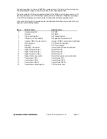
The data acquisition circuitry on ELEKTRA occupies a block of 16 bytes in I/O memory space.
The default address range for this block is 280h – 28Fh (base address 280).
The data acquisition FPGA can be enabled/disabled in the BIOS under the Advanced menu, I/O
devices. Scroll down to the “FPGA Mode:” option and select “Enabled” or “Disabled” accordingly.
If the FPGA is disabled you will not be able to interact with the data acquisition circuit.
A functional list of registers is provided below, and detailed bit definitions are provided on the next
page and in the following chapter.
Base +
Write Function
Read Function
0
Command register
A/D LSB
1
Not
used
A/D
MSB
2
A/D channel register
A/D channel register
3
A/D gain and scan settings
A/D gain and status read back
4
Interrupt / DMA / counter control
Interrupt / DMA / counter control read back
5
FIFO threshold
FIFO threshold read back
6
D/A LSB
FIFO current depth
7
D/A MSB + channel no.
Interrupt and A/D channel read back
8
Digital I/O port A output
Digital I/O port A
9
Digital I/O port B output
Digital I/O port B
10
Digital I/O port C output
Digital I/O port C
11
Digital I/O direction control
Digital I/O direction control read back
12
Counter/timer D7-0
Counter/timer D7-0
13
Counter/timer D15-8
Counter/timer D15-8
14
Counter/timer D23-16
Counter/timer D23-16
15
Counter/timer control register FPGA
revision
code


