background image

4

Using Adobe Reader (Windows version)

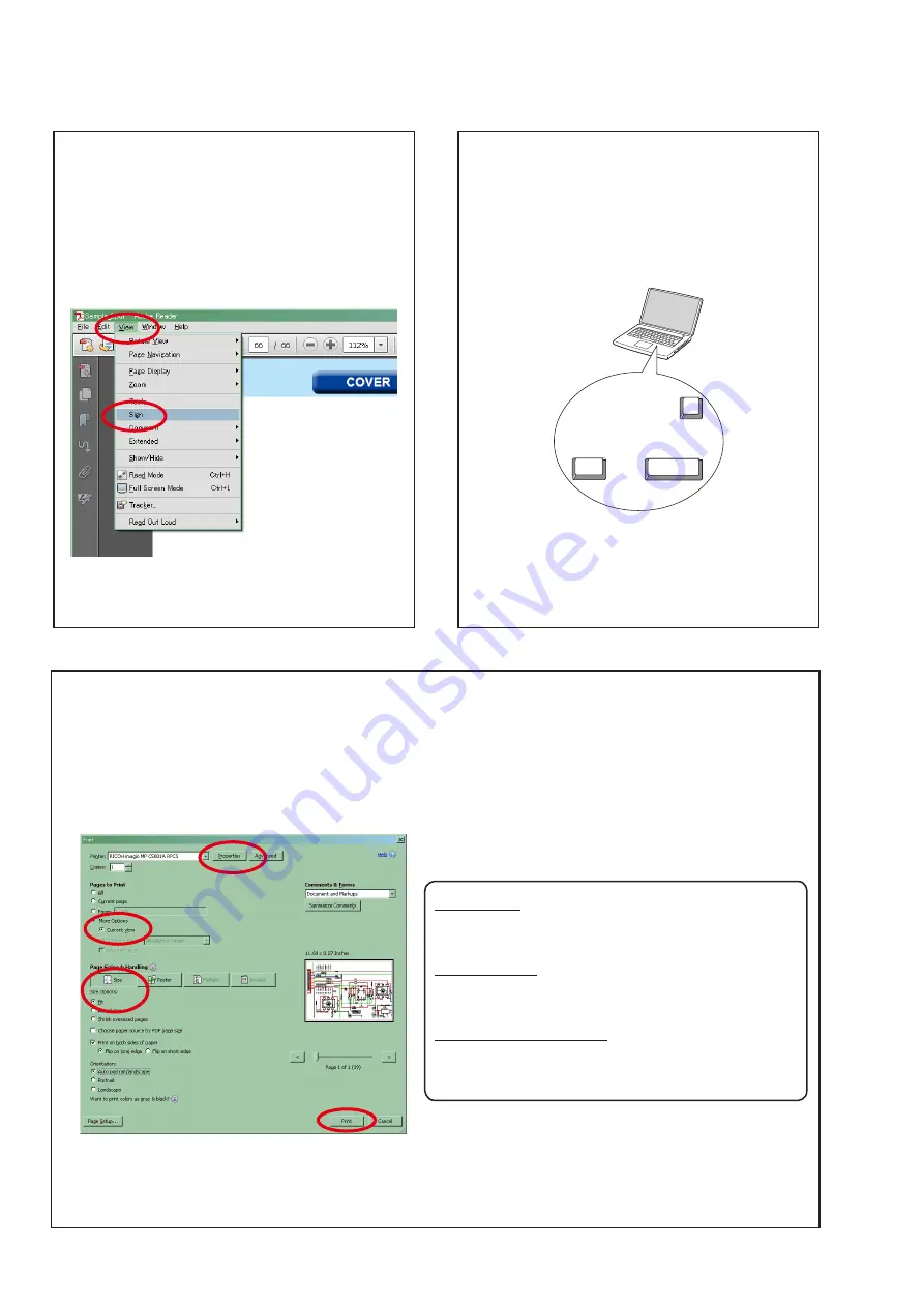
•  Properties 

  Click this button and check that the printer is set to a 

suitable paper size.

•  Page to print 

  Select the following checkbox.

 "

More Options

" : "

Current View

"

•  Page Sizing & Handling 

  Select the following checkbox.

 "

Size

" / "

Size Options

" : "

Fit

"

Add notes to this data (Sign)

The Sign function lets you add notes to the data in this 

manual.

Save the file once you have finished adding notes.

[Example using Adobe Reader X]

On the "

View

" menu, click "

Sign

".

•  The Sign pane appears.

[Example using Adobe Reader 9]

On the "

Document

" menu, click "

Sign

". 

Magnify schematic / printed wiring board 
diagrams - 1
(Ctrl+Space, mouse operation)

Press 

Ctrl

+

Space

  on  the  keyboard  and  drag  the 

mouse to select the area you want to view.

•  The selected area is magnified.

Ctrl

Space

0

•  When you want to move the area shown, hold down 

Space

 and drag the mouse.

•  When  you  want  to  show  a  full  page  view,  press 

Ctrl

+

0

 on the keyboard.

Print a magnified part of the manual

The Properties dialog box and functions will vary depending on your printer.

1. Drag the mouse to magnify the part you want to print.

2. On the "

File

" menu, click "

Print

".

3. Configure the following settings in the Print dialog box.

4. Click the 

Print

 button to start printing.

Содержание CEOL Piccolo DRA-N5

Страница 1: ...Ver 3 S0604 1V03DM DG1212 Some illustrations using in this service manual are slightly different from the actual set Please use this service manual with referring to the operating instructions withou...

Страница 2: ...lay 25 4 Product Mode 1 27 5 Product Mode 2 27 6 Protection history display mode 27 7 DPMS UP date mode 29 8 Update mode by RS232C 31 9 MAC Address rewrite mode 31 10 Access to development server mode...

Страница 3: ...F on the keyboard The Search window appears Ctrl Shift F 2 Enter the Ref No you want to search for in the Search window and then click the Search button A list of search results appears 3 Click an ite...

Страница 4: ...ng Adobe Reader 9 On the Document menu click Sign Magnify schematic printed wiring board diagrams 1 Ctrl Space mouse operation Press Ctrl Space on the keyboard and drag the mouse to select the area yo...

Страница 5: ...reen Example using Adobe Reader 9 On the Tools menu point to Select Zoom and then click Pan Zoom Window Magnify schematic printed wiring board diagrams 3 Loupe Tool function The Loupe Tool function le...

Страница 6: ...ortant safety parts that are indicated by the z mark on schematic diagrams and parts lists be sure to use the designated parts Be sure to mount parts and arrange the wires as they were originally plac...

Страница 7: ...RC Composition RS Metal oxide film RW winding RN Metal film RK Metal mixture P Pulse resistant type NL Low noise type NB Non burning type FR Fuse resistor F Lead wire forming 2B 1 8 W 2E 1 4 W 2H 1 2...

Страница 8: ...perly grounded to remove any static electricity that may be charged on the body 2 Ground for Workbench Be sure to place a conductive sheet or copper plate with proper grounding 1 M on the workbench or...

Страница 9: ...3 Network type wireless LAN standards Conforming to IEEE 802 11b Conforming to IEEE 802 11g Conforming to Wi Fi z Transfer rate DS SS 11 5 5 1 Mbps Automatic switching OFDM 54 48 36 24 18 12 9 6 Mbps...

Страница 10: ...ubstitutes it Initializing NETWORK RECEIVER NETWORK RECEIVER initialization should be performed when the com peripheral parts of com and Digital PCB are replaced 1 Turn off the power using ON STANDBY...

Страница 11: ...Otherwise incorrect arrangement can be a cause of noise generation FRONT PANEL ASSY Refer to DISASSEMBLY 3 FRONT PANEL ASSY and EXPLODED VIEW FRONT PANEL ASSY Ref No of EXPLODED VIEW 2 SMPS PCB ASSY...

Страница 12: ...Shooting direction A B C D Refer to the diagram below about the shooting direction of each photograph Photographs with no shooting direction indicated were taken from the top of the set The photograph...

Страница 13: ...13 1 TOP COVER 1 Remove the screws 2 Remove the screws TOP COVER Proceeding View from the bottom Shooting of photograph A...

Страница 14: ...ER out of the unit toward the back panel 4 Lift up the top cover disconnect the connector wires and remove the screws Shooting of photograph C About 10 mm Shooting of photograph C Shooting of photogra...

Страница 15: ...15 2 MAIN PCB ASSY 1 Cut the clamp bands remove the screws 2 Remove the screws TOP COVER MAIN PCB ASSY Proceeding...

Страница 16: ...iFi Antenna connector USB connector wires 4 Remove the FFC When assembling the parts be aware of the location where FFC passes through the front board and its shape CP301 Shooting of photograph B Shoo...

Страница 17: ...17 5 Remove the MAIN BOARD Shooting of photograph D...

Страница 18: ...the screws 2 Disconnect the connector wires for USB WiFi antenna and headphones and then pull them out of the front plate hole TOP COVER MAIN PCB ASSY FRONT PANEL ASSY Proceeding View from the bottom...

Страница 19: ...19 3 Remove the screws Shooting of photograph D Shooting of photograph C Please refer to EXPLODED VIEW for the disassembly method of FRONT PANEL ASSY...

Страница 20: ...20 4 SMPS PCB ASSY 1 Remove the screws 2 Remove the SHIED SMPS plate TOP COVER MAIN PCB ASSY FRONT PANEL ASSY Proceeding SMPC PCB ASSY Shooting of photograph C...

Страница 21: ...21 3 Remove the screws and the connector wires then disconnect the B D to B D connector CN801 CN224 CNT3 Shooting of photograph D...

Страница 22: ...22 5 AMP PCB ASSY 1 Remove the screws 2 Remove the screws TOP COVER MAIN PCB ASSY SMPS PCB ASSY FRONT PANEL ASSY AMP PCB ASSY Proceeding Shooting of photograph A...

Страница 23: ...the same as the factory initialization Can erase the Recently Played list 3 Version display CURSOR UP Version Display 4 Product mode 1 VOLUME UP CURSOR RIGHT Cooling FAN Select Digital In Function FAN...

Страница 24: ...display All lights on display And light the Power LED White 2 seconds All lights on display And light the Power LED Red Green 2 seconds Factory Reset displayed for 5 seconds Initialization Items Defau...

Страница 25: ...failed log not cleared History of protection not cleared Startup display Initialized displayed for 5 seconds 3 Version display Menu items appear in the Add Version Otherwise normal operation To exit...

Страница 26: ...the Setup Press 1 3 ENTER button The version of the System u com Press Cursor i The version of the boot loader System u com Press Cursor i The version of the display u com Press Cursor i The version o...

Страница 27: ...utes Auto Standby 4 minutes Sleep setting and timer started Auto Standby to set up and will stand under the following conditions Auto Standby Conditions USB iPod No Connection or Unsupported Data or c...

Страница 28: ...or 12V_A or 29V fail Over current Over current detection digital amplifier Protection history is reset When the Cursor u button is pressed for over 5 seconds while the protection history is displayed...

Страница 29: ...of Error code Coping strategies 10 Firm Info response acquisition TimeOut Main rewrite Firmware recived failure TimeOut Turn off and on the power Updating starts automatically 11 Firm Info response ac...

Страница 30: ...s automatically Carry out the update in an environment that has little network load 3D Failed to acquire the IP Address after transitioning to the Boot Loader Mode AutoIP Turn off and on the power Upd...

Страница 31: ...ection Carry out the update in an environment that has little network load AB After download request Login Failed Check the network connection Carry out the update in an environment that has little ne...

Страница 32: ...aced A Mask ROM With software No need write in of software to the microprocessor B Flash ROM With software Usually no need write in of software But when the software was updated you should be write in...

Страница 33: ...ess Cursor u i buttons select to Check for Update Press 1 3 ENTER button 3 Press the 1 3 ENTER button The latest version of the firmware uploaded to the web is displayed If the latest firmware version...

Страница 34: ...EL CS EL_RESET END Check Power Supply Voltages for Main com MAIN B D 5V_SMPS1 CN410 4 5pin 3 3V_CPU IC402 4pin Check Soldering IC402 on MAIN B D CN410 4 5pin on MAIN B D CN005 4 5pin on B D to B D CNT...

Страница 35: ...AIN B D CN410 4 5pin 5V_SMPS1 on MAIN B D CN005 4 5pin 5V_SMPS1 on B D to B D CNT1 CN006 9 10pin 5V_SMPS1 on B D to B D CNT1 CN224 9 10pin 5V_SMPS1 on SMPS B D CP413 1pin 3V3_D1 on MAIN B D CN001 1pin...

Страница 36: ...Check Soldering XTAL102 on AMP B D IC103 20pin 5508_MCLK on AMP B D Check Soldering MAIN B D IC403 86 87 88 89pin MAIN B D DIR_DO DIR_DI DIR_CL DIR_CE NG NG OK OK END Check control signal for PWM CON...

Страница 37: ...8 4 6 14 16pin Check Output of Audio Data from AMP to Speaker AMP B D IC118 22 25 30 33pin JACK105 Check Soldering IC108 on AMP B D Check Soldering IC118 on AMP B D Check Soldering IC118 on AMP B D JA...

Страница 38: ...ck Soldering JACK101 1pin 3V3_D1 on AMP B D IC401 IN 5V_SMPS1 OUT 3V3_D1 on MAIN B D CN410 4 5pin 5V_SMPS1 on MAIN B D CN005 4 5pin 5V_SMPS1 on B D to B D CNT1 CN006 9 10pin 5V_SMPS1 on B D to B D CNT...

Страница 39: ...DIF Check Soldering CN410 1 2 3pin 5V_NET 5V_SMPS2 on MAIN B D CN005 1 2 3pin 5V_D on B D to B D CNT1 CN006 11 12 13pin 5V_D on B D to B D CNT1 CN224 11 12 13pin 5V on SMPS B D Check Soldering CP301 1...

Страница 40: ...40 Personal notes...

Страница 41: ...bwoofer Out AMP SW Power Source Cursor Up Cursor Down Cursor Right Cursor Left Enter Vol Up Vol Down RJ 45 IC108 PWM PROCESSOR TAS5508 IC118 D Amp TAS5142 SPK OUT L SPK OUT R IC103 DIR PCM9211 MUTE I2...

Страница 42: ...CM9211 3 3V_D1 MXS4035A 3 3V_D1 JACK101 JSR1165 C 3 3V_5508 IC108 TAS5508 Q406 5V_VBUS 5V_VBUS LD601 KRA102S IC301 5V_VBUS 5V_VBUS IC310 NCP380 5V_VBUS 5V_VBUS NCP380 Q303 5V_NET USB_VBUS IC306 KRA102...

Страница 43: ...P_ON 07 5508_PDN 08 5508_MUTE 09 GND_AD 10 5508_SDA 11 5508_SCL 12 NC 13 GND_AD 14 DIR_INT 15 DIR_RERR 16 DIR_DO 17 DIR_DI 18 DIR_CL 19 DIR_CE 20 DIR_RST 21 GND_AD 01 GND_D 02 GND_D 03 NET3 3V 04 RXD0...

Страница 44: ...SP_PROTECT 4 5142_SD 9 5V_SMPS1 10 GND_A 7 DC_PROTECT2 3 FAN_ON 5 5142_OTW GND_AD AMP 21 AMUTE 18 H P_ON 20 GND_AD 19 5508_RESET 16 5508_MUTE 17 5508_PDN 11 GND_AD 9 DIR_RERR 10 DIR_INT 12 H P_DET 14...

Страница 45: ...A GND_A GND_A D_GND 12V_D GND_A PROT_CONT TEMP_DET GND_A 12V_A 5142_OTW SP_PROTECT DC_PROTECT2 TEMP_DET FAN_H NC FAN_H FAN_ON 5142_SD 5142_OTW FAN_ON 5V_SMPS1 DC_PROTECT2 H P_DET LEFT GND_A D_GND GND_...

Страница 46: ...16V_OLED CLP403 ZTT12 00MT 5508_RESET DIR_DI 5508_SCL DRA N5 MAIN PCB MP NCP300LSN30T1G NCP380HMU15AATBG CX870_SPDIF D403 R378 L311 R415 R413 R436 R377 C374 D307 D306 D308 C361 R432 R301 R470 R522 R48...

Страница 47: ..._SPDIF CNT2 23P CN002 23P CN001 GND_AD 7 DIR_DI DIR_DO DIR_CL DIR_CE DIR_RST GND_AD 5508_SDA 5508_SCL H P_DET GND_AD DIR_INT H P_ON 5508_PDN GND_AD 3V3_D1 H P_MUTE CX870_SPDIF 5508_RESET 5508_MUTE DRA...

Страница 48: ...FFC CP405 2 4 1 3 CP403 4P FFC R491 OPEN R508 100K R497 4K7 R496 4K7 R498 OPEN 1N C433 C434 10 16 10N C435 TRST TMS IPOD_DET GND_D 3V3_D1 EMLE R444 1K R452 22 R448 22 R459 22 R458 220 R456 33 OPEN R4...

Страница 49: ...GND NET_ 1V9 L316 BLM21PG221 ETH_TXP GND GPIO10 GPIO08 GND USBVBUSDRV AV4DATA1 R349 33 1608 TXD1 AV2CTRL1 AV2CLK VIN 1 2V GND L317 BLM21PG221 L311 BD221JT 100N K C362 CX870_SPDIF USB DATA E_RXDMOEI 12...

Страница 50: ...E GND_5508 C138 100N K C137 100N K C136 100N K 100N K C139 C134 10N K 100 16 C135 OPEN KRC107S Q109 DC_PROTECT2 5508_SCL 3 3V_D1 R153 22 Q110 KRC102S 3 3V_5508 3 3V_D2 R193 2K2 R190 2K2 Q114 KRC102S D...

Страница 51: ...644 OPEN 100 6 3 D642 D643 C647 OPEN D632 KDS4148U KDS4148U D631 C650 100N K C651 10N Z C652 1N K GND_D 1 2 3 4 4P_WIRE SHIELD CP632 EL_DC EL_RST 1000N Z C668 R663 0 3 3V_D1_ L662 BLM11A121 BLM11A121...

Страница 52: ..._A R188 100K 12V_D S603 C604 100N K S607 S605 S604 DOWN 100N K C605 S609 VR_UP R615 150 H P_L 12V_A 12V_A GND_A GND_D 0 1608 R618 GND_A TEMP_DET 5142_OTW 5142_SD NC FAN_ON GND_AD GND_AD L601 BD221 201...

Страница 53: ...SD102M AC250V C826 SD102M AC250V C451 104K 2012 C451 104K 2012 L222 4 7uH AL04 L222 4 7uH AL04 CN222 C125Z1 11 CN222 C125Z1 11 1 2 3 4 5 6 7 8 9 10 11 HSD221 MH 4506 30 HSD221 MH 4506 30 D822 BAV21W D...

Страница 54: ...50 17 51 52 S1 4 S1 4 S1 2 S1 2 S1 1 S1 1 S2 2 S1 1 S1 1 S1 3 S1 1 S1 1 S1 1 S6 1 S1 1 S1 1 S1 1 S1 3 S1 4 S1 4 S5 1 S1 4 S1 8 S1 2 S1 4 S1 1 S1 2 S4 4 S3 6 S1 1 S5 2 S6 1 S1 1 S1 1 S1 2 S6 1 EXPLODED...

Страница 55: ...e supplied P W B ASS Y for which nsp is indicated on this table cannot be supplied When repairing the P W B ASS Y check the board parts table and order replacement parts The parts listed below are for...

Страница 56: ...56 PACKING VIEW 13 11 2 3 1 6 4 5 SET FRONT 9 7 23 E2 10 8 15 19 16 14 20 E3 21 22 27 26 25 12 20 JP 28 17 WHITE 17 WHITE 24...

Страница 57: ...n a separate file See the part list in Excel format TENTATIVE Parts for which nsp is indicated on this table cannot be supplied The parts listed below are for maintenance only might differ from the pa...

Страница 58: ...ORS Only major semiconductors are shown general semiconductors etc are omitted to list The semiconductor which described a detailed drawing in a schematic diagram are omitted to list 1 IC s R5F56108VN...

Страница 59: ...R W WR O O L O L O L EL Writing 29 P30 EL CS O O L O L O L EL Chip Select L I F communication 30 P27 D7 O O L O L O L Data Bus for OLED 31 P26 D6 O O L O L O L Data Bus for OLED 32 P25 D5 O O L O L O...

Страница 60: ...S5142 Shutdown Signal 85 PB1 5142_OTW PU I I I I TAS5142 Overtemperature Warning Signal 86 P74 DIR_DO I I I I PCM9211 DIR Control 87 P73 DIR_DI O O L O L O L PCM9211 DIR Control 88 P72 DIR_CL O O L O...

Страница 61: ...PCB mode 128 P92 LED_WT PU O O L O L O L Control White LED POWER ON H 129 P91 LED_RED PD O O H O H O L Control Red LED ECO STBY L 130 VSS VSS GND 131 P90 LED_GREEN PD O O L O H O L Control Green LED E...

Страница 62: ...62 PCM9211 AMP IC103...

Страница 63: ...63 PCM9211 Block Diagram...

Страница 64: ...64 PCM9211 Pin Discriptions...

Страница 65: ...ND_C 24 30 P Power ground for half bridge C GND_D 23 29 P Power ground for half bridge D GVDD_A 36 44 P Gate drive voltage supply requires 0 1 F capacitor to AGND GVDD_B 1 1 P Gate drive voltage suppl...

Страница 66: ...nd I O Logic PWM_C OUT_C GND_C PVDD_C BST_C Timing Gate Drive Ctrl PWM Rcv GVDD_C PWM_B OUT_B GND_B PVDD_B BST_B Timing Gate Drive Ctrl PWM Rcv GVDD_B PWM_A OUT_A GND_A PVDD_A BST_A Timing Gate Drive...

Страница 67: ...5 V Pullup Headphone in out selector When a logic low is applied the headphone is selected speakers are off When a logic high is applied speakers are selected headphone is off LRCLK 26 DI 5 V Serial a...

Страница 68: ...xternal devices VR_DIG 33 P Voltage reference for 1 8 V digital core supply A pinout of the internally regulated 1 8 V power used by digital core logic A 4 7 F low ESR capacitor 3 should be connected...

Страница 69: ...ds DC Block De Emph SRC NS PWM 0 Det 7 Biquads DRC Loud Comp Soft Tone DC Block De Emph SRC NS PWM 8 2 Crossbar Mixer 0 Det 7 Biquads DRC Loud Comp Soft Tone DC Block De Emph SRC NS PWM 0 Det 7 Biquad...

Страница 70: ...70 L6565 SMPS IC821 L6565 Block Diagram...

Страница 71: ...71 ICE3BR1765J SMPS IC871 ICE3BR1765J Block Diagram...

Страница 72: ...72 2 DISPLAY S020 MXS4035A 3 DISPLAY CP661...

Страница 73: ...rate file See the part list in Excel format TENTATIVE bParts indicated by nsp on this table cannot be supplied bThe parts listed below are only for maintenance Therefore they might differ from the par...

Отзывы: