1. IC's
SEMICONDUCTORS
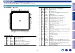
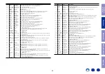
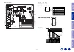
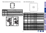
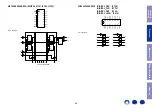
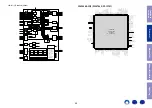
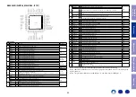
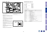
ADV7623 (DIGITAL_OSD : IC731)
ADV7623
TOP VIEW
(Not to Scale)
PIN 1
1
DDCC_SCL
2
3
4
5
6
7
8
9
10
11
12
13
14
15
16
17
18
19
20
21
22
23
24
25
26
27
28
29
30
31
32
33
34
35
36
73
DVDDIO
74
AP3_IN
75
AP2_IN
76
AP1_IN
77
AP0_IN
78
SDATA
79
SCL
80
DGND
81
DVDD
82
INT1
83
INT2
84
INT_TX
85
DGNDIO
86
DVDDIO
87
AP0_OUT
88
AP1_OUT
89
AP2_OUT
90
AP3_OUT
91
AP4_OUT
92
DGND
93
DVDD
94
AP5_OUT
95
SCLK_OUT
96
MCLK_OUT
97
RESET
98
PWRDN
99
PGND
100
PVDD
101
XTAL
102
XTAL1
103
PVDD
104
PGND
105
HP_CTRLA
106
5V_DETA
107
RTERM
108
DDCA_SDA
10
9
11
0
11
1
11
2
11
3
11
4
11
5
11
6
11
7
11
8
11
9
12
0
12
1
12
2
12
3
12
4
12
5
12
6
12
7
12
8
12
9
13
0
13
1
13
2
13
3
13
4
13
5
13
6
13
7
13
8
13
9
14
0
14
1
14
2
14
3
14
4
DD
C
C_
SD
A
37
TX
PL
VD
D
38
TX
G
N
D
39
TX
PG
N
D
40
41
42
43
44
45
46
47
48
49
50
51
52
53
54
55
56
57
58
59
60
61
62
63
64
65
66
67
68
69
70
71
72
EX
T_
SW
IN
G
H
PD_ARC
–
A
RC
+
TX
D
DC
_S
D
A
TX
D
D
C_
SC
L
TX
A
VD
D
TX
G
N
D
TX
C
–
TX
C
+
TX
G
N
D
TX
0–
TX
0+
TX
G
N
D
TX
1–
TX
1+
TX
A
VD
D
TX
2–
TX
2+
TX
G
N
D
C
EC
D
G
N
D
D
VD
D
A
LS
B CS
EP
_S
C
K
EP
_C
S
EP
_M
O
SI
EP
_M
IS
O
M
C
LK
_I
N
SC
LK
_I
N
A
P5_
IN
A
P4_
IN
D
G
N
D
IO
5V
_D
ET
C
H
P_C
TR
LC
R
XB_2
+
R
XB_2
–
TV
D
D
R
XB_1
+
R
XB_1
–
C
G
N
D
R
XB_0
+
R
XB_0
–
TV
D
D
R
XB_C
+
R
XB_C
–
C
G
N
D
C
VD
D
DDCB_
SC
L
DDCB_
SD
A
D
VD
D
D
G
N
D
5V
_D
ET
B
H
P_C
TR
LB
R
XA_2
+
R
XA_2
–
TV
D
D
R
XA_1
+
R
XA_1
–
C
G
N
D
R
XA_0
+
R
XA_0
–
TV
D
D
R
XA_C
+
R
XA_C
–
C
G
N
D
C
VD
D
DDCA_
SC
L
CVDD
CGND
RXC_C–
RXC_C+
TVDD
RXC_0–
RXC_0+
CGND
RXC_1–
RXC_1+
TVDD
RXC_2–
RXC_2+
HP_CTRLD
5V_DETD
DGND
DVDD
DDCD_SDA
DDCD_SCL
CVDD
CGND
RXD_C–
RXD_C+
TVDD
RXD_0–
RXD_0+
CGND
RXD_1–
RXD_1+
TVDD
RXD_2–
RXD_2+
CVDD
CGND
TXPVDD
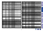
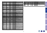
Pin Function Descriptions
Pin No. Mnemonic
Type
Description
1
DDCC_SCL
Digital input
HDCP Slave Serial Clock Port C. DDCC_SCL is a 3.3 V input that is 5 V tolerant.
2
CVDD
Power
Receiver Comparator Supply Voltage (1.8 V).
3
CGND
Ground
TVDD and CVDD Ground.
4
RXC_C−
HDMI input
Digital Input Clock Complement of Port C in the HDMI Interface.
5
RXC_C+
HDMI input
Digital Input Clock True of Port C in the HDMI Interface.
6
TVDD
Power
Receiver Terminator Supply Voltage (3.3 V).
7
RXC_0−
HDMI input
Digital Input Channel 0 Complement of Port C in the HDMI Interface.
8
RXC_0+
HDMI input
Digital Input Channel 0 True of Port C in the HDMI Interface.
9
CGND
Ground
TVDD and CVDD Ground.
10
RXC_1−
HDMI input
Digital Input Channel 1 Complement of Port C in the HDMI Interface.
11
RXC_1+
HDMI input
Digital Input Channel 1 True of Port C in the HDMI Interface.
12
TVDD
Power
Receiver Terminator Supply Voltage (3.3 V).
Pin No. Mnemonic
Type
Description
13
RXC_2−
HDMI input
Digital Input Channel 2 Complement of Port C in the HDMI Interface.
14
RXC_2+
HDMI input
Digital Input Channel 2 True of Port C in the HDMI Interface.
15
HP_CTRLD
Digital output
Hot Plug Detect for Port D.
16
5V_DETD
Digital input
5 V Detect Pin for Port D in the HDMI Interface.
17
DGND
Ground
DVDD Ground.
18
DVDD
Power
Digital Supply Voltage (1.8 V).
19
DDCD_SDA
Digital I/O
HDCP Slave Serial Data Port D. DDCD_SDA is a 3.3 V input/output that is 5 V tolerant.
20
DDCD_SCL
Digital input
HDCP Slave Serial Clock Port D. DDCD_SCL is a 3.3 V input that is 5 V tolerant.
21
CVDD
Power
Receiver Comparator Supply Voltage (1.8 V).
22
CGND
Ground
TVDD and CVDD Ground.
23
RXD_C−
HDMI input
Digital Input Clock Complement of Port D in the HDMI Interface.
24
RXD_C+
HDMI input
Digital Input Clock True of Port D in the HDMI Interface.
25
TVDD
Power
Receiver Terminator Supply Voltage (3.3 V).
26
RXD_0−
HDMI input
Digital Input Channel 0 Complement of Port D in the HDMI Interface.
27
RXD_0+
HDMI input
Digital Input Channel 0 True of Port D in the HDMI Interface.
28
CGND
Ground
TVDD and CVDD Ground.
29
RXD_1−
HDMI input
Digital Input Channel 1 Complement of Port D in the HDMI Interface.
30
RXD_1+
HDMI input
Digital Input Channel 1 True of Port D in the HDMI Interface.
31
TVDD
Power
Receiver Terminator Supply Voltage (3.3 V).
32
RXD_2−
HDMI input
Digital Input Channel 2 Complement of Port D in the HDMI Interface.
33
RXD_2+
HDMI input
Digital Input Channel 2 True of Port D in the HDMI Interface.
34
CVDD
Power
Receiver Comparator Supply Voltage (1.8 V).
35
CGND
Ground
TVDD and CVDD Ground.
36
TXPVDD
Power
1.8 V Power Supply for Digital and I/O Power Supply. This pin supplies power to the
digital logic and I/Os. It should be filtered and as quiet as possible.
37
TXPLVDD
Power
1.8 V Power Supply.
38
TXGND
Ground
TXPVDD Ground.
39
TXPGND
Ground
TXPLVDD Ground.
40
EXT_SWING
Analog input
This pin sets the internal reference currents. Place an 887 Ω resistor (1% tolerance) between
this pin and ground.
41
HPD_ARC−
Analog input
Hot Plug Detect Signal. This pin indicates to the interface whether the receiver is connected.
It supports 1.8 V to 5 V CMOS logic levels.
42
ARC+
Analog input
Audio Return Channel Input (5 V Tolerant).
43
TXDDC_SDA Digital I/O
Serial Port Data I/O to Receiver. This pin serves as the master to the DDC bus. It supports a
5 V CMOS logic level.
44
TXDDC_SCL
Digital output
Serial Port Data Clock to Receiver. This pin serves as the master clock for the DDC bus.
It supports a 5 V CMOS logic level.
45
TXAVDD
Power
1.8 V Power Supply for TMDS Outputs.
46
TXGND
Ground
TXAVDD Ground.
47
TXC−
HDMI output
Differential Clock Output. Differential clock output at the TMDS clock rate; supports
TMDS logic level.
48
TXC+
HDMI output
Differential Clock Output. Differential clock output at the TMDS clock rate; supports
TMDS logic level.
49
TXGND
Ground
TXAVDD Ground.
50
TX0−
HDMI output
Differential Output Channel 0 Complement. Differential output of the red data at 10×
the pixel clock rate; supports TMDS logic level.
51
TX0+
HDMI output
Differential Output Channel 0 True. Differential output of the red data at 10× the pixel clock
rate; supports TMDS logic level.
52
TXGND
Ground
TXAVDD Ground.
53
TX1−
HDMI output
Differential Output Channel 1 Complement. Differential output of the red data at 10×
the pixel clock rate; supports TMDS logic level.
54
TX1+
HDMI output
Differential Output Channel 1 True. Differential output of the red data at 10× the pixel
clock rate; supports TMDS logic level.
55
TXAVDD
Power
1.8 V Power Supply for TMDS Outputs.
Only major semiconductors are shown, general semiconductors etc. are omitted to list.
The semiconductor which described a detailed drawing in a schematic diagram are omitted to list.
42
Caution in
servicing
Electrical
Mechanical
Repair Information
Updating
Содержание AVR-S730H
Страница 148: ...www denon com ...

