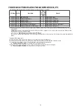
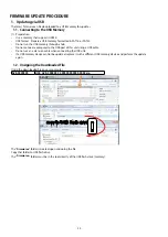
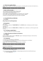
background image

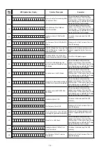
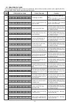
Error 

Code

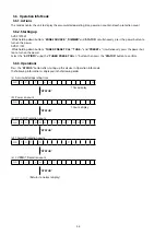
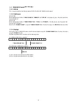
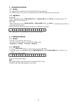
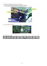
USB Update Error Display

Details of Error code

Remedies

3C

U p d a t i n g

f a i l

3 C

Error notification received while 

requesting the Firmware Info.

This unit automatically retries the 

request several times. Wait until the 

Display stops.  If the Display stops at the 

Error display, press and hold the "Power 

operation" button for 5 seconds.

3D

U p d a t i n g

f a i l

3 D

Time Out while obtaining Firm-

ware information.

This unit automatically retries the 

request several times. Wait until the 

Display stops.  If the Display stops at the 

Error display, press and hold the "Power 

operation" button for 5 seconds.

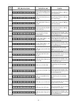
3F

C o n n e c t i o n F a i l 3 F

Failed to transit to SBL Mode.

This unit automatically retries the 

request several times. Wait until the 

Display stops.  If the Display stops at the 

Error display, press and hold the "Power 

operation" button for 5 seconds.

50

C o n n e c t i o n F a i l 5 0

Unable to detect USB.

Disconnect and reconnect the USB 

memory.

51

C o n n e c t i o n F a i l 5 1

No Firmware File in USB.

Make sure that the Firmware File is in 

the USB memory.

52

N o t M a t c h F i r m

5 2

The Firmware File in the USB does 

not support your model and area.

Make sure that the model name and 

area are supported by the Firmware 

File.

54

U p d a t i n g

f a i l

5 4

Error notification received while 

requesting the Firmware Info.

This unit automatically retries the 

request several times. Wait until the 

Display stops.  If the Display stops at the 

Error display, press and hold the "Power 

operation" button for 5 seconds.

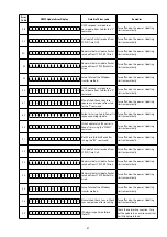
55

U p d a t i n g

f a i l

5 5

Time Out while obtaining Firm-

ware information.

This unit automatically retries the 

request several times. Wait until the 

Display stops.  If the Display stops at the 

Error display, press and hold the "Power 

operation" button for 5 seconds.

56

C o n n e c t i o n F a i l 5 6

Unable to detect USB for Firm-

ware Download.

Disconnect and reconnect the USB 

memory.

57

F i l e s N o t F o u n d

5 7

No Firmware File for Firmware 

Download.

Make sure that the Firmware File is in 

the USB memory.

5A

C o n n e c t i o n F a i l 5 A

Invalid DeviceID in response or 

no response from Sub for the "C" 

command.

This unit automatically retries the 

request several times. Wait until the 

Display stops.  If the Display stops at the 

Error display, press and hold the "Power 

operation" button for 5 seconds.

5B

U p d a t i n g

f a i l

5 B

NACK received in response or 

no response from Sub for the "L" 

command.

This unit automatically retries the 

request several times. Wait until the 

Display stops.  If the Display stops at the 

Error display, press and hold the "Power 

operation" button for 5 seconds.

5C

U p d a t i n g

f a i l

5 C

No Update Packet received from 

CY920 (Time Out).

This unit automatically retries the 

request several times. Wait until the 

Display stops.  If the Display stops at the 

Error display, press and hold the "Power 

operation" button for 5 seconds.

5D

U p d a t i n g

f a i l

5 D

Abnormal data in Update Packet 

received from CY920 (CRCError).

This unit automatically retries the 

request several times. Wait until the 

Display stops.  If the Display stops at the 

Error display, press and hold the "Power 

operation" button for 5 seconds.

5E

U p d a t i n g

f a i l

5 E

Abnormal data in Update Packet 

received from CY920 (PacketNo-

Error).

This unit automatically retries the 

request several times. Wait until the 

Display stops.  If the Display stops at the 

Error display, press and hold the "Power 

operation" button for 5 seconds.

59

Содержание AVR-S710W

Страница 1: ...ease use this service manual with referring to the operating instructions without fail Some illustrations using in this service manual are slightly different from the actual set For purposes of improvement specifications and design are subject to change without notice e SERVICE MANUAL e D M Holdings Inc ...

Страница 2: ...n Mode 25 3 Selecting the Mode for Service related Operations 26 DIAGNOSTIC PATH DIAGRAM 29 4 Remote ID Setup Mode 48 5 Protection Pass Mode 49 6 CY920 Reboot Mode 49 7 CY920 Initialization Mode 50 JIG FOR SERVICING 51 PROCEDURE AFTER REPLACING THE MICROPROCESSOR ETC 53 FIRMWARE UPDATE PROCEDURE 54 1 Updating via USB 54 2 Updating via DPMS 63 ADJUSTMENT 70 SURROUND MODES AND PARAMETERS 71 TROUBLE ...

Страница 3: ... you can do with this manual Search for a Ref No phrase Ctrl Shift F You can use the search function in Acrobat Reader to search for a Ref No in schematic diagrams printed wiring circuit diagrams block diagrams and parts lists 1 Press Ctrl Shift F on the keyboard The Search window appears 2 Enter the Ref No you want to search for in the Search window and then click the Search button A list of sear...

Страница 4: ...g Adobe Reader 9 On the Document menu click Sign Magnify schematic printed circuit board diagrams 1 Ctrl Space mouse operation Press Ctrl Space on the keyboard and drag the mouse to select the area you want to view The selected area is magnified When you want to move the area shown hold down Space and drag the mouse When you want to show a full page view press Ctrl 0 on the keyboard Ctrl Space 0 P...

Страница 5: ...een Example using Adobe Reader 9 On the Tools menu point to Select Zoom and then click Pan Zoom Window Magnify schematic printed circuit board diagrams 3 Loupe Tool function The Loupe Tool function lets you magnify a specific part of a diagram in a separate window Example using Adobe Reader X On the View menu point to Zoom and then click Loupe Tool The Loupe Tool window appears on the screen Examp...

Страница 6: ...tant safety parts that are indicated by the z mark on schematic diagrams and parts lists be sure to use the designated parts Be sure to mount parts and arrange the wires as they were originally placed For safety seasons some parts use tapes tubes or other insulating materials and some parts are mounted away from the surface of printed circuit boards Care is also taken with the positions of the wir...

Страница 7: ... part make a clear distinction between 1 and I i to avoid mis supplying 3 A part ordered without specifying its part number can not be supplied 4 Part indicated by mark is not illustrated in the exploded view WARNING Parts indicated by the z mark have critical characteristics Use ONLY replacement parts recommended by the manufacturer INSTRUCTIONS FOR HANDLING SEMI CONDUCTORS AND OPTICAL UNIT Elect...

Страница 8: ...8 Personal notes ...

Страница 9: ...rd Conforming to IEEE 802 11b Conforming to IEEE 802 11g Conforming to IEEE 802 11n Wi Fi compliant z1 Security WEP 64 bit WEP 128 bit WPA WPA2 PSK AES WPA WPA2 PSK TKIP Radio frequency 2 4 GHz No of channels 1 11 ch for E3 1 13 ch for E2 E1C JP z1 The Wi Fi CERTIFIED Logo and the Wi Fi CERTIFIED On Product Logo are registered trademarks of the Wi Fi Alliance n n Bluetooth section Communications s...

Страница 10: ... 13 9 16 344 1 3 4 45 2 3 8 60 1 3 4 45 9 16 15 5 3 8 136 5 15 16 151 8 7 16 215 11 5 16 288 13 3 8 339 3 4 19 1 1 4 32 7 3 4 197 1 3 4 44 1 7 8 47 DIMENSION FOR AVR X1200W Unit in mm Weight 18 lbs 12 oz 8 5 kg 10 ...

Страница 11: ...ing to IEEE 802 11b Conforming to IEEE 802 11g Conforming to IEEE 802 11n Wi Fi compliant z1 Security WEP 64 bit WEP 128 bit WPA WPA2 PSK AES WPA WPA2 PSK TKIP Radio frequency 2 4 GHz No of channels 1 11 ch z1 The Wi Fi CERTIFIED Logo and the Wi Fi CERTIFIED On Product Logo are registered trademarks of the Wi Fi Alliance n n Bluetooth section Communications system Bluetooth Version 2 1 EDR Enhance...

Страница 12: ... 9 16 15 5 3 8 136 5 15 16 151 8 7 16 215 13 9 16 344 2 3 8 60 1 3 4 45 1 3 4 45 11 5 16 288 13 3 8 339 3 4 19 1 1 4 32 7 3 4 197 1 3 4 44 1 3 4 47 DIMENSION FOR AVR S710W Unit in mm Weight 18 lbs 12 oz 8 5 kg 12 ...

Страница 13: ...unit fails to enter the service mode in step 3 repeat the procedure from step 1 Initializing the device restores the customized settings to the factory settings Write down your settings in advance and reconfigure the settings after initialization AVR X1200W JIG FOR SERVICING Use the following jigs extension cable kit when repairing the PCBs Order with your dealer for the jigs your dealer if necess...

Страница 14: ...he service mode in step 3 repeat the procedure from step 1 Initializing the device restores the customized settings to the factory settings Write down your settings in advance and reconfigure the settings after initialization AVR S710W JIG FOR SERVICING Use the following jigs extension cable kit when repairing the PCBs Order with your dealer for the jigs your dealer if necessary 8U 110084S EXTENSI...

Страница 15: ...P PCB Ref No of EXPLODED VIEW P 12 PHONE WIRE GUIDE PCB Ref No of EXPLODED VIEW P 17 DIGITAL PCB ASSY See DISASSEMBLY 2 DIGITAL PCB ASSY and EXPLODED VIEW DIGITAL PCB Ref No of EXPLODED VIEW P 13 CY920 MODULE Ref No of EXPLODED VIEW P 14 TUNER PCB Ref No of EXPLODED VIEW P 15 TRANS POWER See DISASSEMBLY 6 TRANS POWER and EXPLODED VIEW TRANS POWER Ref No of EXPLODED VIEW P 16 POWER PCB See DISASSEM...

Страница 16: ... indicate the shooting directions of photos The photographs with no shooting direction indicated were taken from the top of the unit Photos of AVR S710W E3 are used in this manual The viewpoint of each photograph Shooting direction X View from the top Front side Shooting direction A Shooting direction B Shooting direction D Shooting direction C 16 ...

Страница 17: ...d connector wires Remove the FFC 2 DIGITAL PCB Proceeding TOP COVER DIGITAL PCB 1 Remove the screws 2 Remove the CORD HOLDERs and connector wires Remove the FFC Remove the screws View from the bottom x5 FFC FFC CN804 CN102 CN104 x1 Shooting direction A x8 x6 FFC FFC CN804 CN823 CN741 CN762 CN822 CN761 x2 CORD HOLDER x 3 17 ...

Страница 18: ...See EXPLODED VIEW for instructions on removing the POWER PCB 5 REGULATOR PCB Proceeding TOP COVER REGULATOR PCB See EXPLODED VIEW for instructions on removing the REGULATOR PCB 6 TRANS POWER Proceeding TOP COVER TRANS POWER See EXPLODED VIEW for instructions on removing the transformer TRANS Shooting direction A x5 x12 x2 x2 x2 x4 CN502 CN104 18 ...

Страница 19: ... See page 47 2 5 Operation Info Mode Displays the accumulated operating time of the unit the number of times the power was switched on and the number of occur rences of each protection See page 46 3 User Initialization Mode TUNER PRESET CH TUNER PRESET CH Initializes backup data Settings for the Installer Setup are not initialized 4 Factory Initialization Mode ZONE2 SOURCE DIMMER Initializes backu...

Страница 20: ...s the accumulated operating time of the unit the number of times the power was switched on and the number of occurrenc es of each protection See page 46 3 User Initialization Mode TUNER PRESET CH TUNER PRESET CH Initializes backup data Settings for the Installer Setup are not initialized 4 Factory Initialization Mode TUNER PRESET CH TUNE Initializes backup data The settings for the Installer Setup...

Страница 21: ...on e Main µ com r Main 1st Boot Loader t DSP ROM y Audio PLD u Video PLD i GUI SFLASH o Ethernet 1st Boot Loader Hardware ID Q0 Ethernet 2nd Boot Loader Rhapsody Flag Q1 Ethernet IMAGE Q2 Ethernet MAC ADDRESS information Q3 BT MAC Address information q Model destination information FLD A V R S 7 1 0 W E 3 FLD A V R X 1 2 0 0 W E 3 FLD A V R X 1 2 0 0 W E 2 FLD A V R X 1 2 0 0 W E 1 C FLD A V R X 1...

Страница 22: ...der Rhapsody Flag FLD E t h e r n e t S B L Press STATUS button FLD B 0 A Q1 Ethernet IMAGE FLD E t h e r n e t I M G Press STATUS button FLD I Q2 Ethernet MAC ADDRESS information FLD N E T M A C A d d r e s s Press STATUS button FLD Q3 BT MAC ADDRESS information FLD B T M A C A d d r e s s Press STATUS button FLD 22 ...

Страница 23: ...ported by the GUI Serial Flash ADV8003 G U I V E R E R R O R Check the firmware version e DIR NG This error is displayed if there is no re sponse from the DIR D I R E R R O R 0 1 Check the DIR U1040 HDMI PCB and sur rounding circuits r DSP NG The DSP FLAG0 port does not enter Hi status while booting a DSP code even after resetting DSP D S P E R R O R 0 1 Check the DSP IC781 DIGITAL PCB and surroun...

Страница 24: ...nformation are written in the Service Information General Firmware Version XXXX XXXX XXXX GUI Image Main Sub 0 0 3 8 Info display 1 2 0 0 8 3 8 2 6 7 7 3 DSP X X 0 2 A PLD V PLD X X 0 1 X X 0 7 GUI X X X X 0 0 1 6 X X X 0 0 0 2 8 E FBL X X X X X X E SBL B X X X X X X X X X X X X E IMG I X X X X X X X X 0 0 3 7 The 1st digit from the right for DSP The 1st digit from the right for A PLD The 1st digi...

Страница 25: ...ode The information shown on the display switches each time the TUNER PRESET CH button is pressed Press the STATUS button to set the currently displayed mode and restart the device The setting with is selected for each mode q FLD F P V O L L O C K O N The buttons on the unit and the master volume knob does not function w FLD F P L O C K O N The buttons on the unit does not function e FLD F P L O C...

Страница 26: ...information shown on the display switches each time the TUNER PRESET CH button is pressed Press the STATUS button to set the currently displayed mode and restart the device q FLD 1 S E R V I C E C H E C K Service Path Check Mode The Video and Audio paths can be checked This function is convenient for confirming problem paths in the product and checking the paths after repairing w FLD 2 P R O T E C...

Страница 27: ...The input source can be switched to any source except CBL SAT 2 DIGITAL MAIN A 0 2 D I G I T A L Input Source CBL SAT Input Mode DIGITAL fixed Sound mode MULTI CH STEREO Amp assign Surround Back Speaker Config ALLSpeaker Small SW Yes 2ch MAIN ZONE ON ZONE2 OFF Digital input Speaker output Front L R Center Surround L R Surround Back L R Digital input Pre output Front L R Center Surround L R Surroun...

Страница 28: ... SAT 3 HDMI CEC Control Monitor HDMI Monitor1 V 0 4 H D M I C E C Input Source CBL SAT HDMI Control ON Control Monitor Monitor1 if checking the HDMI Monitor Out1 MAIN ZONE ON ZONE2 OFF When the power supply of a TV is put in the standby mode make sure that the power supply of this unit is also put in the standby mode b The input source can be switched to any source except CBL SAT The ARC path can ...

Страница 29: ...AT MIC AUTOSETUP NETWORK SW1 MUTE AUDYSSEY MEDIA PLAYER P AMP ZONE2 AVR X1200WE3 ONLY MUTE DA_FL DA_FR DA_CEN DA_SW DA_SL DA_SR DA_SBL DA_SBR ANA_FL ANA_FR H P L GND H P R H P OUT SBL SBR BD3812F VOL IC SW2 DA_SBL DA_SBR FL H FL B BI AMP FL ZONE FL FR H FR B BI AMP FR ZONE FR 32 768kHz FM AM DA01 DA02 DA03 DA04 DA05 DA06 DA03 DA04 DA05 DA06 DA07 DA08 ANA01 DA07 DA08 DA01 DA02 ANA01 ANA02 fig 01 29...

Страница 30: ...L FLASH 256M HDMI TX MN864788 COAX 1 DACFS DAC64FS DAC256FS 5M80ZT100C5N AUDIOPLD TXFS TXI2S0 TX64FS 64FSDIR1 256FSDIR1 FSDIR1 MCLK1 SBCK SLRCK DATADIR1 AUDIO1 DIR1PERR RX256FS RX64FS RXFS RXI2SO HDMI_SPDIF Z2_NET_R ANT1 ANT2 HDMI_SPDIF DIR_CE DIR_DIN DIR_DOUT DIR_CLK DIR_RST From To MCU DAC_MUTE DAC_MS DAC_DATA DAC_RST DAC_CLK From MCU DSP_MISO DSP_CLK DSP_MOSI DSP_RST From To MCU DSP_CS HDMI RX ...

Страница 31: ...IC AUTOSETUP NETWORK SW1 MUTE AUDYSSEY MEDIA PLAYER P AMP ZONE2 AVR X1200WE3 ONLY MUTE DA_FL DA_FR DA_CEN DA_SW DA_SL DA_SR DA_SBL DA_SBR ANA_FL ANA_FR H P L GND H P R H P OUT SBL SBR BD3812F VOL IC SW2 DA_SBL DA_SBR FL H FL B BI AMP FL ZONE FL FR H FR B BI AMP FR ZONE FR 32 768kHz FM AM DA01 DA02 DA03 DA04 DA05 DA06 DA03 DA04 DA05 DA06 DA07 DA08 ANA01 DA07 DA08 DA01 DA02 ANA01 ANA02 31 ...

Страница 32: ...L FLASH 256M HDMI TX MN864788 COAX 1 DACFS DAC64FS DAC256FS 5M80ZT100C5N AUDIOPLD TXFS TXI2S0 TX64FS 64FSDIR1 256FSDIR1 FSDIR1 MCLK1 SBCK SLRCK DATADIR1 AUDIO1 DIR1PERR RX256FS RX64FS RXFS RXI2SO HDMI_SPDIF Z2_NET_R ANT1 ANT2 HDMI_SPDIF DIR_CE DIR_DIN DIR_DOUT DIR_CLK DIR_RST From To MCU DAC_MUTE DAC_MS DAC_DATA DAC_RST DAC_CLK From MCU DSP_MISO DSP_CLK DSP_MOSI DSP_RST From To MCU DSP_CS HDMI RX ...

Страница 33: ...ETUP NETWORK SW1 MUTE AUDYSSEY MEDIA PLAYER P AMP ZONE2 AVR X1200WE3 ONLY MUTE DA_FL DA_FR DA_CEN DA_SW DA_SL DA_SR DA_SBL DA_SBR ANA_FL ANA_FR H P L GND H P R H P OUT SBL SBR BD3812F VOL IC SW2 DA_SBL DA_SBR FL H FL B BI AMP FL ZONE FL FR H FR B BI AMP FR ZONE FR 32 768kHz FM AM DA01 DA02 DA03 DA04 DA05 DA06 DA03 DA04 DA05 DA06 DA07 DA08 ANA01 DA07 DA08 DA01 DA02 ANA01 ANA02 fig 03b 33 ...

Страница 34: ...L FLASH 256M HDMI TX MN864788 COAX 1 DACFS DAC64FS DAC256FS 5M80ZT100C5N AUDIOPLD TXFS TXI2S0 TX64FS 64FSDIR1 256FSDIR1 FSDIR1 MCLK1 SBCK SLRCK DATADIR1 AUDIO1 DIR1PERR RX256FS RX64FS RXFS RXI2SO HDMI_SPDIF Z2_NET_R ANT1 ANT2 HDMI_SPDIF DIR_CE DIR_DIN DIR_DOUT DIR_CLK DIR_RST From To MCU DAC_MUTE DAC_MS DAC_DATA DAC_RST DAC_CLK From MCU DSP_MISO DSP_CLK DSP_MOSI DSP_RST From To MCU DSP_CS HDMI RX ...

Страница 35: ...IC AUTOSETUP NETWORK SW1 MUTE AUDYSSEY MEDIA PLAYER P AMP ZONE2 AVR X1200WE3 ONLY MUTE DA_FL DA_FR DA_CEN DA_SW DA_SL DA_SR DA_SBL DA_SBR ANA_FL ANA_FR H P L GND H P R H P OUT SBL SBR BD3812F VOL IC SW2 DA_SBL DA_SBR FL H FL B BI AMP FL ZONE FL FR H FR B BI AMP FR ZONE FR 32 768kHz FM AM DA01 DA02 DA03 DA04 DA05 DA06 DA03 DA04 DA05 DA06 DA07 DA08 ANA01 DA07 DA08 DA01 DA02 ANA01 ANA02 35 ...

Страница 36: ...L FLASH 256M HDMI TX MN864788 COAX 1 DACFS DAC64FS DAC256FS 5M80ZT100C5N AUDIOPLD TXFS TXI2S0 TX64FS 64FSDIR1 256FSDIR1 FSDIR1 MCLK1 SBCK SLRCK DATADIR1 AUDIO1 DIR1PERR RX256FS RX64FS RXFS RXI2SO HDMI_SPDIF Z2_NET_R ANT1 ANT2 HDMI_SPDIF DIR_CE DIR_DIN DIR_DOUT DIR_CLK DIR_RST From To MCU DAC_MUTE DAC_MS DAC_DATA DAC_RST DAC_CLK From MCU DSP_MISO DSP_CLK DSP_MOSI DSP_RST From To MCU DSP_CS HDMI RX ...

Страница 37: ...IC AUTOSETUP NETWORK SW1 MUTE AUDYSSEY MEDIA PLAYER P AMP ZONE2 AVR X1200WE3 ONLY MUTE DA_FL DA_FR DA_CEN DA_SW DA_SL DA_SR DA_SBL DA_SBR ANA_FL ANA_FR H P L GND H P R H P OUT SBL SBR BD3812F VOL IC SW2 DA_SBL DA_SBR FL H FL B BI AMP FL ZONE FL FR H FR B BI AMP FR ZONE FR 32 768kHz FM AM DA01 DA02 DA03 DA04 DA05 DA06 DA03 DA04 DA05 DA06 DA07 DA08 ANA01 DA07 DA08 DA01 DA02 ANA01 ANA02 37 ...

Страница 38: ...ETUP NETWORK SW1 MUTE AUDYSSEY MEDIA PLAYER P AMP ZONE2 AVR X1200WE3 ONLY MUTE DA_FL DA_FR DA_CEN DA_SW DA_SL DA_SR DA_SBL DA_SBR ANA_FL ANA_FR H P L GND H P R H P OUT SBL SBR BD3812F VOL IC SW2 DA_SBL DA_SBR FL H FL B BI AMP FL ZONE FL FR H FR B BI AMP FR ZONE FR 32 768kHz FM AM DA01 DA02 DA03 DA04 DA05 DA06 DA03 DA04 DA05 DA06 DA07 DA08 ANA01 DA07 DA08 DA01 DA02 ANA01 ANA02 fig 06 38 ...

Страница 39: ...N2 HDMI IN3 AUX CBL SAT HDMI RX MN864788A P3 RX P2 RX P1 RX P0 RX P1 TX AD8195 Buffer MEDIA PLAYER GAME HDMI IN4 HDMI IN5 HDMI TX MN864788 P3 RX P1 RX P0 RX P0 TX P1 TX ADV7623 TRANSCEIVER 28 6363MHz X7201 S FLASH 32M 64M OTHER 32M E1 64M CEA 861 V0 V7 PCLKIN CY920 AVRS710W X1200WVIDEOBLOCK OSD Block P1 RX P0 RX HDMI OUT MONITOR OUT P2 RX RXA 27 000MHz 27 000MHz fig 07 39 ...

Страница 40: ...N2 HDMI IN3 AUX CBL SAT HDMI RX MN864788A P3 RX P2 RX P1 RX P0 RX P1 TX AD8195 Buffer MEDIA PLAYER GAME HDMI IN4 HDMI IN5 HDMI TX MN864788 P3 RX P1 RX P0 RX P0 TX P1 TX ADV7623 TRANSCEIVER 28 6363MHz X7201 S FLASH 32M 64M OTHER 32M E1 64M CEA 861 V0 V7 PCLKIN CY920 AVRS710W X1200WVIDEOBLOCK OSD Block P1 RX P0 RX HDMI OUT MONITOR OUT P2 RX RXA 27 000MHz 27 000MHz fig 08 40 ...

Страница 41: ... IN3 AUX CBL SAT HDMI RX MN864788A P3 RX P2 RX P1 RX P0 RX P1 TX AD8195 Buffer MEDIA PLAYER GAME HDMI IN4 HDMI IN5 HDMI TX MN864788 P3 RX P1 RX P0 RX P0 TX P1 TX ADV7623 TRANSCEIVER 28 6363MHz X7201 S FLASH 32M 64M OTHER 32M E1 64M CEA 861 V0 V7 PCLKIN CY920 AVRS710W X1200WVIDEOBLOCK OSD Block P1 RX P0 RX HDMI OUT MONITOR OUT P2 RX RXA 27 000MHz 27 000MHz fig 09 CEC IC751 CPU 41 ...

Страница 42: ...AL FLASH 256M HDMI TX MN864788 COAX 1 DACFS DAC64FS DAC256FS 5M80ZT100C5N AUDIOPLD TXFS TXI2S0 TX64FS 64FSDIR1 256FSDIR1 FSDIR1 MCLK1 SBCK SLRCK DATADIR1 AUDIO1 DIR1PERR RX256FS RX64FS RXFS RXI2SO HDMI_SPDIF Z2_NET_R ANT1 ANT2 HDMI_SPDIF DIR_CE DIR_DIN DIR_DOUT DIR_CLK DIR_RST From To MCU DAC_MUTE DAC_MS DAC_DATA DAC_RST DAC_CLK From MCU DSP_MISO DSP_CLK DSP_MOSI DSP_RST From To MCU DSP_CS HDMI RX...

Страница 43: ...N2 HDMI IN3 AUX CBL SAT HDMI RX MN864788A P3 RX P2 RX P1 RX P0 RX P1 TX AD8195 Buffer MEDIA PLAYER GAME HDMI IN4 HDMI IN5 HDMI TX MN864788 P3 RX P1 RX P0 RX P0 TX P1 TX ADV7623 TRANSCEIVER 28 6363MHz X7201 S FLASH 32M 64M OTHER 32M E1 64M CEA 861 V0 V7 PCLKIN CY920 AVRS710W X1200WVIDEOBLOCK OSD Block P1 RX P0 RX HDMI OUT MONITOR OUT P2 RX RXA 27 000MHz 27 000MHz fig 11 43 ...

Страница 44: ...mpedance outside the rating were connected Note A short circuit occurred between the speaker terminals or speakers with an impedance outside the rating were connected If the power is turned on in the abnormal state protection is activated after around 6 seconds and the power is turned off c DC if the last protection is DC FLD P R T D C Cause DC output of the power amplifier is abnormal If the powe...

Страница 45: ... P R O T E C T b Initialize this unit See Initializing This Unit on page 13 b Use the method in 3 5 1 if you do not want to erase your settings from this unit Warning Displays by POWER LED If the power is turned off while a protection is being detected the POWER LED flashes in red to warn you depending on the protection status as follows a ASO DC protection Flashes at 0 5 second intervals 0 25 sec...

Страница 46: ...he power but ton to turn on the power Select the 4 OP INFO using the TUNER PRESET CH button then press the STATUS button to confirm 3 6 3 Operations Press the STATUS button after starting up this device in Operation Info mode The following information is displayed in the following order a Accumulated operating time FLD O P T i m e H Time display STATUS b Power on count FLD P O n T i m e Count disp...

Страница 47: ... but ton to turn on the power Select the 5 TUNER FRQ SET using the TUNER PRESET CH button then press the STATUS button to confirm 3 7 3 Displays Start up this unit in TUNER STEP mode select the desired option using the TUNER PRESET CH button then enter using the STATUS button The following information is displayed in the following order a AM9 kHz FM50 kHz is selected FLD A M 9 F M 5 0 TUNER PRESET...

Страница 48: ... Remote ID Setup mode is activated the following message is displayed FLD R E M O T E I D 2 Press the QUICK SECT1 4 button that corresponds to the number you want to this unit Button Display QUICK SELECT 1 R E M O T E I D 1 QUICK SELECT 2 R E M O T E I D 2 QUICK SELECT 3 R E M O T E I D 3 QUICK SELECT 4 R E M O T E I D 4 3 Press the power button to turn off the power 4 Press the power button to tu...

Страница 49: ...ay message after the following is displayed FLD P r o t e c t i o n P a s s This is displayed for 5 seconds before returning to the normal display 6 CY920 Reboot Mode 6 1 Actions The CY920 is restarted after CY920 hang up The CY920 can be restarted even in the network standby setting Setup menu Network IP Control Always On 6 2 Operations 1 Turn the MAIN ZONE button on and set the input source to N...

Страница 50: ...s on hold down buttons ZONE2 SOURCE and DIMMER for at least 3 seconds AVR S710W While the power is on hold down buttons TUNER PRESET CH and TUNE for at least 3 seconds Initializing Display FLD I n i t i a l i z i n g FLD I n i t i a l i z i n g FLD I n i t i a l i z i n g FLD I n i t i a l i z i n g Complete Display FLD C o m p l e t e d This is displayed for 5 seconds before returning to the norm...

Страница 51: ... your dealer if necessary CAUTION Incorrect connections may cause malfunction Connection of Jig for HDMI PCB Items to Be Prepared 8U 110084S EXTENSION UNIT KIT 1Sets Insulation sheet Not supplied 1 sheet Ground lead Not supplied 2 pc 手順 1 Remove the screws 2 Remove the connector PCB Shooting direction A x8 x6 CN822 x2 51 ...

Страница 52: ...ath the HDMI PCB b Connect the earth of the PCB to the chassis using an earth wire etc 4 Connect the expansion cables Board to Board Connections No Pin Ref No PCB Ref No PCB q 15pin CN201 DIFF AMP CN822 DIGITAL PCB DIGITAL Insulation sheet CHASSIS HDMI CONNECTOR CHASSIS COMPOSIT CONNECTOR DIFF AMP DIGITAL 1 52 ...

Страница 53: ...lay if the DIGITAL PCB or the CY920 is replaced as this results in the version of the INTERNAL ROM differing from that of the EXTERNAL ROM In this case see Update Procedure in the Event of a CY920 Error This does not require special operations such as pushing multiple buttons at the same time The firmware also cannot be updated via DPMS Procedure after Replacement A The software has been written T...

Страница 54: ...t of this unit using a USB cable Do not use an extension cable when connecting the USB unit If a USB memory device cannot be updated replace it with a different USB memory device and perform the update again 1 2 Unzipping the Downloaded File Unzip the downloaded file on your computer AVR XXXXXXX USB_AVR XXXXXXX_XXXXXXXXXXXX XXXX zip The firmwares folder is created upon unzipping the file Copy that...

Страница 55: ...mory into the USB port NOTE Remove the LAN cable from this unit when performing updates 1 5 Start the update AVR X1200W While holding down buttons TUNER PRESET CH and STATUS simultaneously press the power button to turn on the power AVR S710W While holding down buttons ZONE2 SOURCE and TUNE simultaneously press the power button to turn on the power 1 6 Display during USB update After around half m...

Страница 56: ...taneously insert the AC plug to turn the power on AVR S710W While holding down buttons the ZONE2 SOURCE and TUNE buttons simultaneously insert the AC plug to turn the power on 1 9 3 The firmware update finishes Returns to the normal status after update is completed 1 10 Update Procedure in the Event of a CY920 Error 1 10 1 Actions Perform the following update procedure if CY920 Error appears in th...

Страница 57: ... d 0 B No Firmware File for Firmware Download Make sure that the Firmware File is in the USB memory 0C C o n n e c t i o n F a i l 0 C Received value with the invalid Package Version This unit automatically retries the request several times Wait until the Display stops If the Display stops at the Error display press and hold the Power operation button for 5 seconds 10 U p d a t i n g f a i l 1 0 N...

Страница 58: ... n n e c t i o n F a i l 2 5 Failed to transit to SBL Mode This unit automatically retries the request several times Wait until the Display stops If the Display stops at the Error display press and hold the Power operation button for 5 seconds 26 D o w n l o a d f a i l 2 6 Time Out in Download writing to SDRAM for Firmware Download This unit automatically retries the request several times Wait un...

Страница 59: ...atically retries the request several times Wait until the Display stops If the Display stops at the Error display press and hold the Power operation button for 5 seconds 56 C o n n e c t i o n F a i l 5 6 Unable to detect USB for Firm ware Download Disconnect and reconnect the USB memory 57 F i l e s N o t F o u n d 5 7 No Firmware File for Firmware Download Make sure that the Firmware File is in ...

Страница 60: ...ral times Wait until the Display stops If the Display stops at the Error display press and hold the Power operation button for 5 seconds 81 U p d a t i n g f a i l 8 1 Block Erase failed in Read after issuing the BE command This unit automatically retries the request several times Wait until the Display stops If the Display stops at the Error display press and hold the Power operation button for 5...

Страница 61: ...for Firmware Download This unit automatically retries the request several times Wait until the Display stops If the Display stops at the Error display press and hold the Power operation button for 5 seconds B1 C o n n e c t i o n F a i l B 1 Time Out in Download writing to SDRAM for Firmware Download This unit automatically retries the request several times Wait until the Display stops If the Disp...

Страница 62: ...P L D m i n 50 52 54 57 5A 64 DSP L1 D S P m i n 50 52 54 57 5A 64 GUI Serial Flash L1 G U I m i n 50 52 54 57 5A 62 64 80 86 CY920 second Boot Loader L1 E S B L m i n A2 A4 A6 A7 AE AF B1 B5 CY920 Image L1 E I M G m i n A2 A4 A6 A7 AE AF B1 B5 CY920 Image Emergency Mode L1 U p d a t e r e t r y Checking the Firmware Version After the Update After updating the firmware check the version See 1 Vers...

Страница 63: ...stalled press the SETUP button to exit the menu 4 Select Start using the cursor buttons and then press ENTER The power display lights in red and the GUI screen display disappears during the update The remaining time of the update is shown on the display of the unit Returns to the normal status after the update is completed Cautions on Firmware Update For the update procedure a proper broadband Int...

Страница 64: ...ent that has little network load 08 C o n n e c t i o n F a i l 0 8 Error notification received while requesting the Firmware Info Check the network connection Carry out the update in an environment that has little network load 09 C o n n e c t i o n F a i l 0 9 Time Out while obtaining Firm ware information Check the network connection Carry out the update in an environment that has little networ...

Страница 65: ...s little network load 22 L o g i n f a i l e d 2 2 DPMS login incorrect notification after SBL Initialize the unit and try updating again Carry out the update in an environment that has little network load 23 S e r v e r i s b u s y 2 3 DPMS congestion notification after SBL Carry out the update in an environment that has little network load 24 C o n n e c t i o n F a i l 2 4 DPMS connection failu...

Страница 66: ... i l e d 5 0 DPMS login incorrect notification Carry out the update in an environment that has little network load 51 S e r v e r i s b u s y 5 1 DPMS congestion notification Carry out the update in an environment that has little network load 52 C o n n e c t i o n F a i l 5 2 DPMS connection failure notifica tion Check the network connection Carry out the update in an environment that has little ...

Страница 67: ... t i n g f a i l 6 2 Failed to start up Sub in Power On sequence during Update Turn off and on the power Updating starts automatically 80 U p d a t i n g f a i l 8 0 Write Enable Latch Bit not set in Read after issuing the WREN command Turn off and on the power Updating starts automatically 81 U p d a t i n g f a i l 8 1 Block Erase failed in Read after issuing the BE command Turn off and on the p...

Страница 68: ...irmware Down load Turn off and on the power Updating starts automatically Carry out the update in an environment that has little network load AF D o w n l o a d f a i l A F Error Server Busy notification re ceived while requesting Firmware Download Turn off and on the power Updating starts automatically Carry out the update in an environment that has little network load B0 D o w n l o a d f a i l ...

Страница 69: ... A P L D m i n 50 52 54 58 5A 62 DSP L1 D S P 1 m i n 50 52 54 58 5A 62 GUI Serial Flash L1 G U I m i n 50 52 54 58 5A 62 80 86 CY920 second Boot Loader L1 E S B L m i n A0 A4 A6 A7 AE B5 CY920 Image L1 E I M G m i n A0 A4 A6 A7 AE B5 CY920 Image Emergency Mode L1 U p d a t e r e t r y Checking the Firmware Version After the Update After updating the firmware check the version See 1 Version Displa...

Страница 70: ...ch CN550 CENTER ch CN530 SURROUND Lch CN520 SURROUND Rch CN540 SURROUND BACK Lch CN560 SURROUND BACK Rch CN570 3 Connect the power cord to an outlet Next press the power button to turn on the power 4 Set this unit as follows MASTER VOLUME c min turn counterclockwise to the lowest position SPEAKER Speaker terminal No load Do not connect equipment such as speakers or dummy resistors MODE MCH STEREO ...

Страница 71: ... S S S S Multi Ch In S S S S Dolby Surround S S S S S S DTS Neural X S S S S S Dolby Digital S S S S S S Dolby Digital Plus S S S S S S Dolby TrueHD S S S S S S Dolby Atmos S S S S S S DTS Surround S S S S S DTS 96 24 S S S S DTS HD S S S S DTS Express S S S S DTS X S S S S S S Multi Ch Stereo S S S S S S Rock Arena S S S S S S Jazz Club S S S S S S Mono Movie S S S S S S Video Game S S S S S S Ma...

Страница 72: ...is set to On 8 This item cannot be set when Audyssey Setup Speaker Calibration has not been performed 9 This item cannot be set when MultEQ XT is set to Off 10 This item can be set when the input signal is analog PCM 48 kHz or 44 1 kHz Sound mode Surr Parameter Tone z7 Audyssey Restorer z10 Room Size Center Spread DTS Neural X MultEQ XT z8 Dynamic EQ z9 Dynamic Volume z9 Direct Pure Direct 2 chann...

Страница 73: ...channel signal Multi channel signal Analog PCM Dolby Digital HD DTS HD PCM Multi DTS X DTS HD DTS Express DTS ES Dscrt6 1 DTS ES Mtrx6 1 DTS Dolby Atmos Dolby TrueHD Dolby Digital Plus Dolby Digital EX DTS Surround DTS X MSTR DTS X F DTS HD MSTR Fz3 DTS HD HI RES Fz4 DTS ES Dscrt6 1 z2 F DTS ES Mtrx6 1 z2 F DTS Surround S S F DTS 96 24 Fz5 DTS Express F DTS HD Neural X S S S DTS Neural X S F Dolby...

Страница 74: ...rts To 3 5 Protection History Display Mode See page 44 Are there any parts not fully connected into the connec tors that connect the PCBs Is DC5V output even when the connector CN741 supplying power from the SMPS PCB to the DIGITAL PCB is removed Check the circuits around the Microprocessor on the DIGITAL PCB and replace any faulty parts Check for breakages and short circuits in the circuits and p...

Страница 75: ...7216 D7215 D7101 D7128 D7129 D7130 D7201 D7202 D7203 D7204 D7205 D7214 D7212 D7213 D7211 D7210 D7208 D7209 D7207 D7127 D7126 D7125 D7124 D7123 D7122 D7121 D7120 D7117 D7116D7115 D7114D7113 D7112 D7111 D7110 D7103 D7206 D7119 D7118 D7109 D7108D7107 D7104 D7105 D7106 T791 T7139 T7140 T7301 R7236 R7235 R 73 21 R 73 20 R 73 19 L8005 T8017 T7753 T7756 T7755 T7754 T7507 T7508 T7509 T7510 T8009 T8008 T80...

Страница 76: ...fluorescent display lit Proceed to YES when using a Blu ray DVD player produced by other manufactures 9 Is sound output from the speaker terminal of this unit when the power of the TV is turned off or the cable connecting the TV to this unit is removed Check the connection of the HDMI DVI cable Use a certified HDMI cable with the HDMI mark Replace the HDMI DVI cable with the one shorter than 5m 2m...

Страница 77: ... the TV support 1080P 4K Use a TV that supports HDCP Computer moni tors cannot be used Check the instruction manual of the TV and check the input setting The TV is faulty If the TV does not support 1080P 4K a picture cannot be output even if the Blu ray DVD player is set to 1080P 4K NO NO NO NO See AVR X1200W S710W_HDMI Rx Tx Failure Detection Procedure Manual ver_1 00 of SDI 77 ...

Страница 78: ...T Legacy PCM or DolbyDigital or dts CHECK4 INPUT SURROND MODE SOURCE Audio output OK HDMI Legacy PCM2ch or DolbyDigital or dts CHECK6 INPUT Connect AVR s connected in HDMI audio out put OK HDMI This unit s HDMI OUT Other AVR s HDMI IN Setting SURROND MODE SOURCE CEC STANDBY HBR audio DolbyTrueHD or dtsHD MA CHECK5 INPUT SURROND MODE SOURCE Audio output OK HDMI HBR audio DolbyTrueHD or dtsHD MA CHE...

Страница 79: ...trimmer potentiometer between the base of the power transistor open 1k Ω Are any other transistors faulty Are any other resistors faulty Turn on the power and check that the voltage of each part is correct and that there is an idling current Replace the power transistor Replace the transistor Replace the resistor Replace the emitter resistor Replace the base resistor Replace the trimmer potentiome...

Страница 80: ...GITAL PCB CN822 Is the serial data for electronic volume sent to the IC821 of DIGITAL PCB Reconnect the connectors correctly If the malfunctioning channel and function can be identified check the correspond ing signal path Repair the 12V power supply Repair the power amplifier Check the CPU YES NO YES NO YES NO 80 ...

Страница 81: ...orrectly Check the instruction manual of the router and config ure the settings correctly Check that there are no connection restrictions by MAC addresses etc NO NO NO Is the LAN cable correctly inserted Insert the LAN cable correctly and then turn on the power again NO Check the connection environment Checking the unit YES YES Can the D3 3V output voltage 3 3 V to IC741 DC DC Conv be confirmed Ca...

Страница 82: ...ER1 IC751 uCOM 53 pin Hi Is E_POWER3 IC751 uCOM 56 pin Hi Is E_POWER4 IC751 uCOM 61 pin Hi Is E_POWER2 IC751 uCOM 55 pin Hi The circuit of E_POWER1 between Q7404 and IC751 are faulty The circuit of E_POWER3 between IC751 and Q7402 are faulty The circuit of E_POWER4 between IC751 and IC743 are faulty The circuit of E_POWER2 between IC751 and IC741 are faulty The circuit around Q7402 FET SW is fault...

Страница 83: ... correctly Is the Wi Fi BT antenna cable inserted correctly into CY920 Is the Bluetooth device compatible with the A2DP profile Is the Bluetooth function enabled on the Bluetooth device Connect the Wi Fi BT antenna cable correctly Use a device that is A2DP profile compatible Enable the Bluetooth function and try connecting again NO NO NO Checking the unit Check the Bluetooth device being used 83 ...

Страница 84: ...odels Do not use a USB hub NO YES NO Checking the unit YES YES Can a voltage 5V be confirmed between pin 1 and pin 4 of JK101 USB Connector on USB PCB The USB signal circuit between CY920 and JK101 of the USB PCB are faulty Are CN804 of the DIGITAL PCB and BN104 of the USB PCB correctly connected The circuit around IC854 of the DIGITAL PCB is faulty Connect the connectors correctly NO NO 5 3 Canno...

Страница 85: ...CB Check the damaged parts Replace the damaged part Replace the damaged part Is the fuse F6001 functioning prop erly Are there any short circuits caused by the soldering on the PCB Are any parts damaged Replace the IC601 TOP268VG and D6001 D6004 DC 5V is not output YES YES YES YES YES YES 6 SMPS 85 ...

Страница 86: ...18 27V C6008 50V 10UF NXA D6008 1N4007 C6014 0 1uF 1608 C6015 4 7uF 1608 C6017 OPEN C6018 5600uF 6 3V NXA C6019 5600uF 6 3V NXA C6023 2200P 250V C6024 0 1uF 1608 R6017 3 3K 0 2W R6016 C6002 0 01uF 250V C6003 0 01uF 250V R6026 OPEN 1608 C6025 OPEN 1608 C6004 400V 100uF R6031 1M 2125 R6032 1M 2125 R6033 1M 2125 4 3 2 1 IC602 ZD621 7 5V J6002 JUMPER J6003 JUMPER D G S Q6002 INK0010AC1 3 2 1 D6013 RBQ...

Страница 87: ...C8212 C8211 C8210 C8209 C8208 C8206 C8203 C7412 C8024 C8023 C7992 C7991 C7985 C7975 C7965 C7955 C7945 C7935 C7925 C7915 C7910 C7909 C7908 C7479 C7468 C7457 C7445 C7434 C7423 C7523 C7522 C7521 C7520 C8205 C8204 C8202 C8201 C7448 C7470 C7459 C7436 C7905 C7901 C7387 C7383 C7449 C7471 C7460 C7437 C7426 C7416 C7275 C7274 C7273 C 71 62 C7167 C7166 C 71 63 C 71 56 C 71 55 C7516 C8017 C8016 C8000 C7999 C7...

Страница 88: ...SPK OUT H P OUT SW YES DIGITAL GAIN setting of MASTER VOL 00dB SW YES ANALOG SW NONE DIGITAL SW NONE ANALOG 1 Basic OFFSET of VOL 0dB PREAMPGAIN 15 5dB 2 OFFSET of SWNON 3 OFFSET of the AD input 2 5dB 2 5dB 2 5dB 2 5dB 2 5dB 1dB 9 5dB 13dB 1 2 3 MIC IN GAIN ADJ 28 31dB MIC IN 11 48mVrms 0dBFS 3Vpp 1 06Vrms SINGLE INPUT DIFF OUT PREOUT 150mVrms H P OUT 12dB 12dB 3 5dB 3 5dB POWERAMP GAIN ZONE2 SEL ...

Страница 89: ...H STEREO ANA INPUT 200mVrms L R 1kHz FULL SCALE LEVEL 2 0Vrms 3 01dB 2 5dB 1 0dB 4 27Vrms 8ohm SPK OUT DIGITAL IN GAIN setting of MASTER VOL 00dB ANALOGIN 1 Basic OFFSET of VOL 0dB PREAMPGAIN 15 5dB at VOLMAX 2 OFFSET of the AD input ATT 2 5dB 2 5dB 2 5dB 1 0dB 1 2 GAIN ADJ 3 5dB PRE OUT 150mVrms 29dB POWERAMP GAIN 3 01dB NJM8080 MAX OUTPUT 7 78Vrms NJU72340 MAX OUTPUT 3 8Vrms DIFF OUT 0dBFS 4 0Vp...

Страница 90: ... L R 1kHz 2 5dB 1 0dB 29dB DOLBY DIGITAL IN GAIN setting of MASTER VOL 00dB ANALOGIN 2 5dB 2 5dB 2 5dB 1 0dB 1 2 DSP OUTOPUT 23 5dBFS FULL SCALE LEVEL 2 0Vrms 3 01dB POWERAMP GAIN 4 27Vrms 8ohm SPK OUT PRE OUT 150mVrms 1 Basic OFFSET of VOL 0dB PREAMPGAIN 15 5dB at VOLMAX 2 OFFSET of the AD input ATT 3 5dB GAIN ADJ NJM8080 MAX OUTPUT 7 78Vrms NJU72340 MAX OUTPUT 3 8Vrms DSP OUTOPUT 20dBFS DD INPUT...

Страница 91: ...FFSET of the AD input ATT 1 Basic OFFSET of VOL 0dB PREAMPGAIN 15 5dB at VOLMAX ANALOGIN GAIN setting of MASTER VOL 00dB DIGITAL IN SPK OUT 4 27Vrms 8ohm 1 0dB 2 5dB 3 01dB FULL SCALE LEVEL 2 0Vrms ANA INPUT 200mVrms L R 1kHz MODE MULTI CH STEREO DD INPUT 20dBFS SURR B 1kHz 40dBFS 30dBFS 20dBFS 0dBFS 10dBFS PCM1690 DAC 30dB 50dB 20dB 10dB 30dB 40dB 20dB 10dB 200mVrms 0dB 50dB 20dB 10dB 30dB 40dB 2...

Страница 92: ...ER VOL 00dB ANALOGIN 1 Basic OFFSET of VOL 0dB 3 OFFSET of the AD input 2 5dB 2 5dB 1 2 3 3 5dB 12dB 9 5dB 13dB 2 SW ch revision MUTE 9 5dB 13dB 300Vrms 12dB GAIN ADJ 5 01dB NJU72340 MAX OUTPUT 3 8Vrms PCMINPUT 20dBFS L R 30Hz MODE MULTI CH STEREO DSP OUTOPUT 34dBFS 20 20 6 34dB ANA INPUT 200mVrms L R 20Hz MODE MULTI CH STEREO DSP OUTOPUT 37 5dBFS 20 3 5 20 6 37 5dB DSP OUTPUT 40dBFS 9 5dB NJM8080...

Страница 93: ...0A FRONT ZONE2 BD3812F 50dB 0dB 200mVrms 10dB 20dB 40dB 30dB 10dB 20dB 50dB 30dB 29dB 4 27Vrms 8ohm 277mVrms 33ohm SPK OUT GAIN ADJ PREOUT 150mVrms H P OUT POWERAMP GAIN ZONE2 SEL REC INH ANALOG NJU72340 MAX OUTPUT 3 8Vrms NJM8080 MAX OUTPUT 7 78Vrms 18dB 15dB NOT USE ZONE2 OUT 93 ...

Страница 94: ...UTOSETUP NETWORK SW1 MUTE AUDYSSEY MEDIA PLAYER P AMP ZONE2 AVR X1200WE3 ONLY MUTE DA_FL DA_FR DA_CEN DA_SW DA_SL DA_SR DA_SBL DA_SBR ANA_FL ANA_FR H P L GND H P R H P OUT SBL SBR BD3812F VOL IC SW2 DA_SBL DA_SBR FL H FL B BI AMP FL ZONE FL FR H FR B BI AMP FR ZONE FR 32 768kHz FM AM DA01 DA02 DA03 DA04 DA05 DA06 DA03 DA04 DA05 DA06 DA07 DA08 ANA01 DA07 DA08 DA01 DA02 ANA01 ANA02 94 ...

Страница 95: ...LASH 256M HDMI TX MN864788 COAX 1 DACFS DAC64FS DAC256FS 5M80ZT100C5N AUDIO PLD TXFS TXI2S0 TX64FS 64FSDIR1 256FSDIR1 FSDIR1 MCLK1 SBCK SLRCK DATADIR1 AUDIO1 DIR1PERR RX256FS RX64FS RXFS RXI2SO HDMI_SPDIF Z2_NET_R ANT1 ANT2 HDMI_SPDIF DIR_CE DIR_DIN DIR_DOUT DIR_CLK DIR_RST From To MCU DAC_MUTE DAC_MS DAC_DATA DAC_RST DAC_CLK From MCU DSP_MISO DSP_CLK DSP_MOSI DSP_RST From To MCU DSP_CS HDMI RX MN...

Страница 96: ...MI IN6 HDMI IN1 HDMI IN2 HDMI IN3 AUX CBL SAT HDMI RX MN864788A P3 RX P2 RX P1 RX P0 RX P1 TX AD8195 Buffer MEDIA PLAYER GAME HDMI IN4 HDMI IN5 HDMI TX MN864788 P3 RX P1 RX P0 RX P0 TX P1 TX ADV7623 TRANSCEIVER 28 6363MHz X7201 S FLASH 32M 64M OTHER 32M E1 64M CEA 861 V0 V7 PCLKIN CY920 OSD Block P1 RX P0 RX HDMI OUT MONITOR OUT P2 RX RXA 27 000MHz 27 000MHz 96 ...

Страница 97: ...N5339QI 1 8V 1000mA 2273 52mA 110 06mA 20 4mA NJM2595 MCU 5V CVDBLBJEGJ204L FRONT LED 30mA 1232mA SMPS Total Current About 4294 563mA BU33TD3WG 45mA DA 3 3V PCM5100 MM1Z5V1 MM1Z5V1 MM1Z7V5 SN74CBT3251PWR SWM5V 0 003mA 79 62mA 490 43mA INPUT CURRENT Ref Volage 5 2V 183mA NET3 3V NETWORK CY920 MX25L25635FM IPOD AUTH 604mA PLD1 8V PLD 5M80ZT100C5N NET1 8V NETWORK CY920 CS49844A M12L64164A 5TG2Y 5M80Z...

Страница 98: ...NT TRANS MAIN TRANS REGUL 5P 5P MIC FRONT HDMI DIGITAL BN12A BN12B CN102 BN101_1 BN101 5P 27P 27P 9P 9P DIFF AMP PCB CN201 15P CN822 REGULATOR DIGITAL REGULATOR DIGITAL ANT1 ANT2 CY920 PCB TO PCB PCB TO PCB PCB TO PCB PCB TO PCB PCB TO PCB PCB TO PCB PCB TO PCB PCB TO PCB PCB TO PCB 7P 7P 7P 7P 7P 7P 7P REGULATOR PCB 64P 8P 8P CN762 CN761 9P 9P 5P CN804 CN821 CN508 9P 9P BN502 BN501 PCB TO PCB 15P...

Страница 99: ...IC742 R8512 R8511 R 7 1 3 2 L8008 L8007 L8201 L7527 L7526 L7519 L7525 L7524 L7523 L7522 L7521 L7520 L7518 L7517 L7516 L7515 L7514 L7513 L7512 L7511 L7510 L7509 L7508 L7507 L7506 L7505 L7504 L7503 L7502 L7501 L7483 L7429 L7403 L7402 L7401 L7443 L7442 L7463 L7462 L7453 L7451 L7413 L7411 L7306 L7302 L7303 L 7 3 0 4 L7308 L7307 R7539 C7902 C8813 C8812 C7962 C7952 C7942 C7932 C7922 C7912 T 7 3 1 2 T 7 ...

Страница 100: ...SBR 12 AGND 13 SBL 14 AGND 15 12V 1 FB_FR 2 FB_FR 3 PRE_ B 4 PRE_ B 5 FR 6 FR 7 AGND 3 PRE_ B 4 PRE_ B 1 FB_SR 2 FB_SR 5 SR 6 SR 7 AGND 3 PRE_ B 4 PRE_ B 1 FB_CEN 2 FB_CEN 5 CEN 6 CEN 7 AGND 3 PRE_ B 4 PRE_ B 7 AGND 1 FB_SL 2 FB_SL 5 SL 6 SL 3 PRE_ B 4 PRE_ B 7 AGND 1 FB_FL 2 FB_FL 5 FL 6 FL 3 PRE_ B 4 PRE_ B 7 AGND 1 FB_SBR 2 FB_SBR 5 SBR 6 SBR 7 AGND 1 FB_SBL 2 FB_SBL 3 PRE_AGND 4 PRE_AGND 5 SBL...

Страница 101: ...5812 D5813 D5814 D5816 R5330 J5801 RY586 D5606 D5706 D5106 D5206 D5306 D5406 D5506 R5807 R5826 R5632 R5132 R5232 R5332 R5432 R5532 R5732 R5116 R5115 R5216 R5215 R5316 R5315 R5416 R5415 R5516 R5515 R5825 R5824 R5823 R5821 R5801 R5802 R5819 R5117 R5118 R5217 R5218 R5317 R5318 R5417 R5418 R5517 R5518 R5119 R5120 R5121 R5122 R5219 R5220 R5221 R5222 R5319 R5320 R5321 R5322 R5419 R5420 R5421 R5422 R5519...

Страница 102: ... X1200W X520BT PRESET X1200W X520BT PRESET S710W ZONE2 SEL S510BT SOUND X1200W ZONE2 ON OFF X520BT TUNE S510BT S710W PRESET S510BT S710W PRESET X520BT TUNE X1200W ZONE2 SEL X520BT X1200W DIMMER S510BT S710W TUNE X520BT X1200W STATUS S510BT S710W TUNE S710W BAND X520BT X1200W Q S_1 S500BT S700W BAND X510BT X1100W Q S_1 X520BT X1200W Q S_2 S710W MODE S510BT S710W DIMMER X520BT X1200W Q S_3 S510BT S7...

Страница 103: ... A D7101 A A D7102 A A D7103 A A D7104 A A D7105 A A D7106 A A D7107 A A D7108 A A D7109 A A D7110 T7102 T7103 T7104 1 2 3 4 5 6 7 8 9 10 11 12 13 14 15 16 17 18 19 JK701 CJJ9H021Z T7101 Q7101 CVTRT1N141C Q7102 CVTRT1N141C R7105 47K R7106 0 C7101 0 1uF R7101 1K R7102 10K R7103 47K R7104 47K A A D7111 A A D7112 A A D7113 A A D7114 A A D7115 A A D7116 A A D7117 A A D7118 A A D7119 A A D7120 T7112 T7...

Страница 104: ...T1N141C Q7202 CVTRT1N141C R7205 47K R7206 0 C7201 0 1uF R7201 1K R7202 10K R7203 47K R7204 47K A A D7211 A A D7212 A A D7213 A A D7214 A A D7215 A A D7216 A A D7217 A A D7218 A A D7219 A A D7220 T7212 T7213 T7214 1 2 3 4 5 6 7 8 9 10 11 12 13 14 15 16 17 18 19 JK741 CJJ9H021Z T7211 Q7211 CVTRT1N141C Q7212 CVTRT1N141C R7215 47K R7216 0 C7211 0 1uF R7211 1K R7212 10K R7213 47K R7214 47K R7207 0 R720...

Страница 105: ...F L7301 CB03YTYH600 L7302 CB03YTYH600 C7318 0 1uF C7311 10 6 3V L7304 CB03YTYH600 C7312 0 1uF C7313 10 6 3V L7303 CB03YTYH600 C7342 0 1uF C7338 10 6 3V L7308 CB03YTYH600 L7307 CB03YTYH600 C7340 0 1uF C7341 10 6 3V C7327 0 1uF C7328 10 6 3V L7305 CB03YTYH600 L7306 CB03YTYH600 C7325 0 1uF C7326 10 6 3V C7337 0 1uF C7336 0 1uF C7334 0 1uF C7333 0 1uF C7332 0 1uF C7329 0 1uF C7321 OPEN R7308 47K R7325...

Страница 106: ...348K 1 C7459 5PF C7460 1uF 1 2 3 4 5 6 7 8 9 10 11 12 13 14 15 16 17 18 19 20 21 22 23 24 IC745 CVIEN5339QI R7453 100K R7444 348K 1 R7446 169K 1 R7445 0 C7448 5PF C7449 1uF 1 2 3 4 5 6 7 8 9 10 11 12 13 14 15 16 17 18 19 20 21 22 23 24 IC744 CVIEN5339QI R7443 100K C7411 0 1uF C7456 0 1uF C7467 OPEN C7444 0 1uF C7414 22 6 3V C7417 22 6 3V C7418 10 6 3V C7419 22 6 3V C7458 22 6 3V C7461 22 6 3V C746...

Страница 107: ...58 10K R7511 75 R7524 10K R7525 10K 1 2 3 4 5 6 7 8 9 10 11 12 13 14 15 16 IC753 CVIMC14094BDTR2G 1 2 3 4 5 6 7 8 9 10 11 12 13 14 15 16 IC754 OPEN C7518 0 1uF R7535 33 R7547 33 R7549 33 R7550 33 C7519 OPEN R7537 33 R7536 33 T7510 T7509 T7508 T7507 L7528 CB03YTYH600 L7529 CB03YTYH600 L7530 CB03YTYH600 T7506 T7505 T7504 T7503 X7501 12MHz C7503 9P C7504 9P 1 2 3 CN754 R7579 OPEN R7580 33 R7583 10K M...

Страница 108: ...12 4K7 R7611 3K9 R7617 10K Q7602 CVTRT1N141C Q7603 CVTRT1N141C Q7604 CVTRT1N141C R7623 3K9 R7627 22K R7630 22K L7601 CB03YTYH600 L7602 CB03YTYH600 L7603 CB03YTYH600 L7604 CB03YTYH600 L7605 CB03YTYH600 L7606 CB03YTYH600 L7607 CB03YTYH600 L7608 CB03YTYH600 L7609 CB03YTYH600 L7610 CB03YTYH600 L7611 CB03YTYH600 L7612 CB03YTYH600 L7613 CB03YTYH600 L7614 CB03YTYH600 L7615 CB03YTYH600 L7616 CB03YTYH600 L...

Страница 109: ...SS355T D7704 1SS355T D7705 1SS355T R7703 150 C7703 OPEN R7704 150 D7701 OPEN R7705 470 R7708 47K R7710 33 R7709 330K R7706 OPEN R7707 OPEN C7706 0 1uF C7705 0 1uF 14 13 12 11 10 9 8 7 6 5 4 3 2 1 IC771 TC74VHCU04 C7704 0 01uF 1 2 3 4 5 6 7 8 9 10 11 12 13 14 15 16 17 18 19 20 21 22 23 24 25 26 27 28 29 30 31 32 33 34 35 36 37 38 39 40 41 42 43 44 45 46 47 48 49 50 51 52 53 54 55 56 57 58 59 60 61 ...

Страница 110: ...F C7842 1000P C7844 1000P C7838 0 1uF C7839 1000P C7826 0 1uF R7841 33 R7801 33 R7802 33 R7838 33 8 7 6 5 4 3 2 1 IC782 MX25L6406EM2I 12G R7844 33 R7846 10K R7845 OPEN R7849 10K R7842 10K C7830 0 1uF R7847 10K R7843 10K R7848 10K 7 6 5 4 3 2 1 CN781 OPEN CJP07GA333ZR T7802 T7801 T7804 T7803 R7815 33 R7814 33 R7804 33 X7801 24 576MHz R7821 1M C7814 12P C7815 15P R7822 0 R7823 20K 7 6 5 4 3 2 1 CN78...

Страница 111: ...7916 100 63V C7926 100 63V C7993 0 1uF C7994 0 1uF C7995 1000P C7996 1000P C7997 1000P C7998 1000P C7999 1000P C8000 1000P R7905 OPEN R7906 OPEN C7915 OPEN C7925 OPEN C7935 OPEN C7945 OPEN C7955 OPEN C7965 OPEN C7992 0 1uF C7991 0 1uF C7910 0 1uF C7909 0 1uF C7908 0 1uF R7908 0 R7907 0 T794 T795 T792 T793 1 2 3 4 5 6 7 8 9 10 11 12 13 14 15 16 17 18 19 20 21 22 23 24 25 26 27 28 29 30 31 32 33 34 ...

Страница 112: ...1uF C8055 2 2 6 3V C8057 0 1uF C8056 2 2 6 3V R8061 470 R8062 470 C8053 0 1uF C8054 10 6 3V R8060 10K R8055 10K R8059 OPEN R8056 OPEN T8020 T8019 R8063 0 R8064 0 C8022 0 1uF R8058 10K C8012 0 022uF C8058 OPEN 1 2 3 4 5 6 7 8 IC801 CVIBD82065FVJ E2 1 2 3 4 5 6 7 8 9 10 JK801 CJJ9L029Z RJ45 C8009 0 1uF C8007 0 1uF R8018 OPEN T8002 T8003 T8004 T8001 7 6 5 4 3 2 1 CN803 04 6232 007 010 801 CJP07GA333Z...

Страница 113: ...C8240 10 50V R8246 100K R8245 100K Q8501 CVTRT1P441C Q8201 CVTRT1P441C R8258 10K R8515 10K D8206 1SS355T C8259 10 50V R8257 10K D8203 1SS355T D8204 1SS355T R8255 820 R8256 0 D8205 MM1Z3V6 R8242 0 R8513 100 R8514 100 C8821 0 1uF C8820 0 1uF C8822 0 1uF C8216 0 1uF C8215 0 1uF 1 2 3 4 5 6 7 8 9 10 11 12 13 14 15 16 17 18 19 20 21 22 23 24 25 26 27 28 29 30 31 32 33 34 35 36 37 38 39 40 41 42 43 44 4...

Страница 114: ... R5232 10 1W L5201 0 5UH R5225 10K R5227 5 6K R5228 OPEN R5224 180K D5206 1SS133MT R5223 820K R5229 15K R5230 22K R5231 22K C5209 0 1uF R5332 10 1W L5301 0 5UH R5325 10K R5327 5 6K R5328 OPEN R5324 180K D5306 1SS133MT R5323 820K R5329 15K R5330 22K R5331 22K C5309 0 1uF R5432 10 1W L5401 0 5UH R5425 10K R5427 5 6K R5428 OPEN R5424 180K D5406 1SS133MT R5423 820K R5429 15K R5430 22K R5431 22K C5409 ...

Страница 115: ...V R8103 22K R8102 1K C8101 0 1uF R8105 0 R8104 47K R8107 47K R8106 OPEN C8112 10 6 3V C8110 0 1uF C8111 0 1uF C8113 0 1uF C8114 0 1uF C8115 0 1uF C8116 0 1uF C8117 0 1uF C8108 0 1uF C8109 0 1uF C8134 0 01uF R8122 OPEN R8123 4K7 R8124 OPEN R8121 0 R8120 0 R8118 0 R8117 0 R8126 2K R8127 2K R8119 OPEN R8116 OPEN C8119 0 1uF C8120 0 1uF R8109 OPEN R8125 OPEN 20 21 23 22 19 18 16 17 15 14 13 12 11 10 9...

Страница 116: ...C2403 82P R2404 18K R2405 1 2K C2402 470P 100V R2402 680 C2401 47UF 50V J2401 OPEN R2403 10K C2505 220 50V R2509 33K R2508 470K R2507 220 R2511 OPEN R2510 47 1W R2506 1 2K 1W C2506 33P C2504 2200P M C2503 82P R2504 18K R2505 1 2K C2502 470P 100V R2502 680 C2501 47UF 50V J2501 OPEN R2503 10K R2101 100K R2201 100K R2301 100K R2401 100K R2501 100K D2101 OPEN D2201 OPEN D2301 OPEN D2401 OPEN D2501 OPE...

Страница 117: ...OPTION R1071 OPTION SW117 SW113 SW119 SW101 SW106 SW107 SW112 R1076 OPTION R1081 OPTION R1010 39K C1010 10 16V C1011 0 1uF R1012 100 R1013 100 R1014 100 R1015 100 C1015 330P C1014 100P C1013 100P R1018 100 R1019 100 Q1003 2SC3052 Q1004 2SC3052 R1017 100K R1016 100K C1019 10 50V C1020 0 01uF 1 2 3 CN104 C1068 0 1uF C1071 680P C1072 680P R1057 470 1 2 3 7 8 JK104 CJJ2E026Z SILVER SW111 SW118 LUG13 D...

Страница 118: ... 100V D3001 1N4007 D3002 1N4007 D3003 1N4007 D3004 1N4007 C3012 470 50V C3014 OPEN C3007 3300 25V C3015 OPEN C3013 470 50V D3103 1SS133MT C3010 OPEN C3011 OPEN D3104 1SS133MT GND OUT IN 3 2 1 IC305 CVIKIA7805BPI C3002 OPEN C3009 OPEN C3001 OPEN C3008 470 50V D3108 OPEN GND OUT IN 3 2 1 IC301 CVIKIA7812BPI D3101 OPEN C3006 4700 25V C3024 OPEN 5 4 3 2 1 CN302 BK301 3 1 2 OUT IN GND IC302 HVIKIA7912P...

Страница 119: ...007 D6002 1N4007 D6003 1N4007 D6004 1N4007 CX602 OPEN R6013 15K 1608 R6014 2K 1608 R6012 270K R6010 1M 0 2W R6008 2 2M 0 2W ZD608 39V ZD609 39V ZD610 39V R6009 2 2M 0 2W ZD617 22V ZD616 22V ZD615 22V ZD614 22V ZD613 22V ZD612 22V ZD611 22V C6011 1000P 1KV CX601 0 1uF 250V F6001 CY602 470P 250V CY601 470P 250V 2 1 CN602 YW396 NNB C6001 0 01uF 250V R6015 6 8 0 2W C6013 47 25V NXA R6011 10 1608 D6012...

Страница 120: ...1 S1 x1 S1 x1 S4 x1 S11 x3 S7 x1 S8 x2 S7 x1 S1 x1 S1 x1 S12 x14 S4 x2 S12 x7 S4 x2 S7 x4 S6 x3 S9 x3 S9 x3 S4 x2 S2 x2 S6 x1 S3 x2 S6 x1 S3 x2 S3 x6 S6 x5 S3 x2 S6 x7 S6 x3 S6 x1 S14 x1 S14 x1 S2 x4 S5 x2 F14 ONLY BKE3 ONLY S710W P18 S4 x2 P17 P14 S2 x1 F15 z z WARNING Parts marked with this symbol z have critical characteristics Use ONLY replacement parts recommended by the manufacturer Please s...

Страница 121: ...UK plug Adaptor 5 2 5 3 5 4 5 5 5 6 5 7 5 8 5 9 z 6 2 6 3 6 1 5 1 6 9 5 10 8 7 3 1 2 4 11 13 12 12 14 5 10 PACKING VIEW Please see the last chapter for the part list 121 ...

Страница 122: ..._MOSI EP_MISO MCLK_IN SCLK_IN AP5_IN AP4_IN DGNDIO 5V_DETC HP_CTRLC RXB_2 RXB_2 TVDD RXB_1 RXB_1 CGND RXB_0 RXB_0 TVDD RXB_C RXB_C CGND CVDD DDCB_SCL DDCB_SDA DVDD DGND 5V_DETB HP_CTRLB RXA_2 RXA_2 TVDD RXA_1 RXA_1 CGND RXA_0 RXA_0 TVDD RXA_C RXA_C CGND CVDD DDCA_SCL CVDD CGND RXC_C RXC_C TVDD RXC_0 RXC_0 CGND RXC_1 RXC_1 TVDD RXC_2 RXC_2 HP_CTRLD 5V_DETD DGND DVDD DDCD_SDA DDCD_SCL CVDD CGND RXD_...

Страница 123: ...ply This pin supplies power to the digital logic and I Os It should be filtered and as quiet as possible 37 TXPLVDD Power 1 8 V Power Supply 38 TXGND Ground TXPVDD Ground 39 TXPGND Ground TXPLVDD Ground 40 EXT_SWING Analog input This pin sets the internal reference currents Place an 887 Ω resistor 1 tolerance between this pin and ground 41 HPD_ARC Analog input Hot Plug Detect Signal This pin indic...

Страница 124: ...ply This pin supplies power to the digital logic and I Os It should be filtered and as quiet as possible 37 TXPLVDD Power 1 8 V Power Supply 38 TXGND Ground TXPVDD Ground 39 TXPGND Ground TXPLVDD Ground 40 EXT_SWING Analog input This pin sets the internal reference currents Place an 887 Ω resistor 1 tolerance between this pin and ground 41 HPD_ARC Analog input Hot Plug Detect Signal This pin indic...

Страница 125: ... 120 TVDD Power Receiver Terminator Supply Voltage 3 3 V 121 RXA_2 HDMI input Digital Input Channel 2 Complement of Port A in the HDMI Interface 122 RXA_2 HDMI input Digital Input Channel 2 True of Port A in the HDMI Interface 123 HP_CTRLB Digital output Hot Plug Detect for Port B 124 5V_DETB Digital input 5 V Detect Pin for Port B in the HDMI Interface 125 DGND Ground DVDD Ground 126 DVDD Power D...

Страница 126: ...P5_OUT SCLK_OUT MCLK_OUT ARC RX EDID REPEATER CONTROLLER RX HPD CONTROLLER EP_MISO EP_MOSI EP_CS EP_SCK SPI MASTER SLAVE EQUALIZER RXB_0 RXB_1 RXB_2 EQUALIZER SAMPLER SAMPLER RXC_0 RXC_1 RXC_2 EQUALIZER SAMPLER RXD_0 RXD_1 RXD_2 EQUALIZER CEC CONTROLLER EDID RAM SAMPLER HDMI RECEIVER PROCESSOR TRANSMITTER PACKET BUILDER HDCP ENCRYPTION ENGINE HDMI ENCODER SERIALIZER TMDS DRIVERS INT1 INT2 INT_TX I...

Страница 127: ... FET multiplexer demultiple resistance of the switch allows connections to be made with minimal propagation delay When output enable OE is low the SN74CBT3251 is enabled S0 S1 and S2 select on the A input data ORDERING INFORMATION TA PACKAGE ORDERABLE PART NUMBER TOP S MARK QFN RGY Tape and reel SN74CBT3251RGYR CU251 SOIC D Tube SN74CBT3251D CBT32 SOIC D Tape and reel SN74CBT3251DR CBT32 40 C to 8...

Страница 128: ...should be no traces on PCB top layer under these keep out areas NOTE C White dot on top left is pin 1 indicator on top of the device package PIN NAME FUNCTION 1 21 24 NC SW NO CONNECT These pins are internally connected to the common switching node of the internal MOSFETs They must be soldered to PCB but not be electrically connected to any external signal ground or voltage Failure to follow this ...

Страница 129: ...109 110 111 112 113 114 115 116 117 118 119 120 121 122 123 124 125 126 127 128 129 130 131 132 133 134 135 136 137 138 139 140 141 142 143 144 PE0 D8 PD6 D6 PD5 D5 PD4 D4 P64 CS4 B P63 CS3 A CS7 A P62 CS2 A CS6 A P61 CS1 CS2 B CS5 A CS6 B CS7 B P60 CS0 CS4 A CS5 B PD3 D3 PD2 D2 PD1 D1 PD0 D0 P96 AN14 P95 AN13 P94 AN12 P93 AN11 P92 AN10 P91 AN9 VSS P90 AN8 VCC P47 AN7 IRQ15 B P46 AN6 IRQ14 B P45 A...

Страница 130: ... ADV7623 SPI CLK O L L L HDMI transceiver w GUI ADV7623 control pin 47 P10 IRQ0 B ADV7623 SPI CS O L L L HDMI transceiver w GUI ADV7623 control pin 48 P37 PO15 TIOCA2 TIOCB2 TCLKD A HSCL 400k O CEC3VPu L L L HDMI transceiver w GUI ADV7623 control pin 49 P36 PO14 TIOCA2 HSDA 400k I_O CEC3VPu L L L HDMI transceiver w GUI ADV7623 control pin 50 P35 PO13 TIOCA1 TIOCB1 TCLKC A MN864788 RST O SW3VPu L L...

Страница 131: ... PCM9211 control pin 88 P72 DIR DOUT I DA3VPu I I I DIR PCM9211 control pin 89 P71 CS4 C CS5 C CS6 C CS7 C DIR CLK O L L L DIR PCM9211 control pin 90 P70 CS3 B ADTRG2 DIR RST O L L L DIR PCM9211 control pin 91 VCC VCC Power supply pin 92 PB0 A8 PO24 TIOCA9 7623 ROM HOLD O L L L FLASH ROM for GUI control pin 93 VSS VSS Ground pin 94 PA7 A7 PO23 TIOCA8 TIOCB8 TCLKH VEXP OE O L L L EXPANDER MC14094 c...

Страница 132: ... Fluorescent display control pin 123 P97 AN15 DA POWER O L L L DIGITAL AUDIO power supply control pin 124 P96 AN14 CEC POWER O L L CEC STANDBY power supply control 125 P95 AN13 DV POWER1 O L L DIGITAL VIDEO power supply control pin 126 P94 AN12 THERMAL B I SW3VPu I L I PROTECTION detect signal input pin 127 P93 AN11 MAIN POWER O L L L Power supply control pin 128 P92 AN10 CPU POWER O L L L CPU POW...

Страница 133: ...IC 16 Pb Free 48 Units Rail MC14094BDR2G SOIC 16 Pb Free 2500 Units Tape Reel NLV14094BDR2G MC14094BDTR2G TSSOP 16 Pb Free 2500 Units Tape Reel NLV14094BDTR2G MC14094BFELG SOEIAJ 16 Pb Free 2000 Units Tape Reel For information on tape and reel specifications including part orientation and tape sizes please refer to our Tape and Reel Packaging Specifications Brochure BRD8011 D NLV Prefix for Automo...

Страница 134: ...P VIEW RGY PACKAGE TOP VIEW 1 20 10 11 2 3 4 5 6 7 8 9 19 18 17 16 15 14 13 12 2OE 1Y1 2A4 1Y2 2A3 1Y3 2A2 1Y4 1A1 2Y4 1A2 2Y3 1A3 2Y2 1A4 2Y1 1OE 2A1 V GND CC SN74LVC244A OCTAL BUFFER DRIVER WITH 3 STATE OUTPUTS SCAS414X NOVEMBER 1992 REVISED MARCH 2005 65 V to 3 6 V tages to 5 5 V 0 C to 85 C and 40 C to t 3 3 V ut Ground Bounce 0 8 V 25 C put V OH Undershoot 2 V 25 C ode Signal Operation on All...

Страница 135: ...serial audio data input 2 29 RXIN6 ALRCKI0 I Yes Biphase signal input 6 AUXIN0 LR clock input 2 30 RXIN5 ABCKI0 I Yes Biphase signal input 5 AUXIN0 bit clock input 2 31 RXIN4 ASCKI0 I Yes Biphase signal input 4 AUXIN0 system clock input 2 32 RXIN3 I Yes Biphase signal input 3 2 33 RXIN2 I Yes Biphase signal input 2 2 36 35 34 33 32 31 30 29 28 27 26 25 1 2 3 4 5 6 7 8 9 10 11 12 ERROR INT0 NPCM IN...

Страница 136: ...PORT RXIN8 RXIN9 RXIN10 RXIN11 DITOUT AUTO DIR ADC AUXIN0 AUXIN1 AUXIN2 AUTO DIR ADC AUXIN0 AUXIN1 AUXIN2 AUTO DIR ADC AUXIN0 AUXIN1 DIT Lock DIR Unlock ADC AUXIN 2 AUXOUT OSC Divider XMCKO Divider XMCKO DITOUT RECOUT0 RECOUT1 AUXIN 0 AUXIN1 ADC Standalone ADC Mode Control Function Control REGISTER POWER SUPPLY MC SCL MDI SDA MDO ADR0 MS ADR1 FILT PLL DIR Lock Detection ERROR INT0 NPCM INT1 ADC Cl...

Страница 137: ...72 RESET DBDA1 DBCK0 EE_CS0 GPIO1 DAI1_D4 GPIO68 BDI DAI1_D2 GPIO66 BDI DAI1_D1 GPIO65 SD_CS EXT_OE SD_BA0 EXT_A13 SD_CAS EXT_CS2 GND1 VDD2 DAI1_D5 GPIO69 EE_CS1 GPIO0 VDD10 BDI DAI1_D3 GPIO67 VDD1 GND2 TEST_EN SD_BA1 EXT_A14 GND3 BDI DAI1_LRCK1 GPIO70 SD_A10 EXT_A12 DBDA0 DBCK1 GND8 VDD8 SCP1_CS GPIO145 SD_D4 EXT_D12 GND9 SCP_BSY GPIO143_OD DA03_D1 GPIO32 DA03_D5 GPIO34 DAO3_D6 GPIO35 SD_DQM0 EXT...

Страница 138: ...put for 1 x I O Serial Data Output for Dual Output mode ata Output for 1 x I O Serial Data or Dual Output mode put tection o pause the device without ng the device N l for MX25L1606E only 5mm USON 4x4mm 8 PIN SOP 200mil 150mil 8 PIN PDIP 300mil 8 P N PM1548 REV 1 2 JUL 02 2010 BLOCK DIAGRAM 138 ...

Страница 139: ... cycle prior new command Disable input buffers for power down in standby A0 A11 Address Row column address are multiplexed on the same pins Row address RA0 RA11 column address CA0 CA7 BA1 BA0 Bank Select Address Selects bank to be activated during row address latch time Selects bank for read write during column address latch time RAS Row Address Strobe Latches row addresses on the positive going e...

Страница 140: ...t from DAC7 VOUT6 33 O No No Positive analog output from DAC6 VOUT6 34 O No No Negative analog output from DAC6 VOUT5 35 O No No Positive analog output from DAC5 VOUT5 36 O No No Negative analog output from DAC5 VOUT4 37 O No No Positive analog output from DAC4 VOUT4 38 O No No Negative analog output from DAC4 VOUT3 39 O No No Positive analog output from DAC3 VOUT3 40 O No No Negative analog outpu...

Страница 141: ... 8 V at V CC 3 3 V T A 25 C Typical V OHV Output V OH Undershoot 2 V at V CC 3 3 V T A 25 C Supports Mixed Mode Signal Operation on All Ports 5 V Input Output Voltage With 3 3 V V CC I off Supports Partial Power Down Mode Operation Latch Up Performance Exceeds 250 mA Per JESD 17 ESD Protection Exceeds JESD 22 2000 V Human Body Model A114 A 200 V Machine Model A115 A 1000 V Charged Device Model C10...

Страница 142: ...a bit clock input DIN 14 I Audio data input LRCK 15 I Audio data word clock input FMT 16 I Audio format selection I2 S Low Left justified High XSMT 17 I Soft mute control Soft mute Low soft un mute High LDOO 18 Internal logic supply rail terminal for decoupling DGND 19 Digital ground DVDD 20 Digital power supply 3 3V 1 Failsafe LVCMOS Schmitt trigger input 6 Copyright 2011 Texas Instruments Incorp...

Страница 143: ...17 18 19 20 21 24 27 37 Exposed Pad 28 29 31 32 33 34 35 36 38 39 40 1 HS high speed LS low speed I input and O output NOTES 1 THE AD8195 LFCSP HAS AN EXPOSED PAD ON THE UNDERSIDE OF THE PACKAGE THAT AIDS IN HEAT DISSIPATION THE PAD MUST BE ELECTRICALLY CONNECTED TO THE AVEE SUPPLY PLANE IN ORDER TO MEET THERMAL SPECIFICATIONS AD8195 TOP VIEW Not to Scale 1 IN0 2 IP0 3 IN1 4 IP1 5 VTTI 6 IN2 7 IP2...

Страница 144: ...NJU72340AFH3 DIGITAL_ANALOG IC821 NJU72340A Terminal Functions 144 ...

Страница 145: ... gain Frequency Fig 5 Output voltage Input voltage Fig 6 THD N Input voltage Fig 7 Output gain Frequency VCC VEE 0 6 18dB 2dB step NJM2595 1 5 INPUT 3 OUTPUT VIDEO SWITCH GENERAL DESCRIPTION PACKAGE OUTLINE FEATURES 5 input 3 output Operating Voltage 4 0 to 6 5V Operating current 15mAtyp at Vcc 5V Crosstalk 65dBtyp Internal 6dB Amplifier Internal 75Ω Driver Bipolar Technology Package Outline DIP16...

Страница 146: ...control Internal shunt regulator connection to provide internal bias current during normal operation It is also used as the connection point for the supply bypass and auto restart compensation capacitor EXTERNAL CURRENT LIMIT X Pin Input pin for external current limit adjustment remote ON OFF and device reset A connection to SOURCE pin disables all functions on this pin This pin should not be left...

Страница 147: ...2 FL DISPLAY FLD 018BT021GINK FRONT FL101 PIN CONNECTION GRID ASSIGNMENT 147 ...

Страница 148: ...ANODE CONNECTION 148 ...

Страница 149: ...ohm S710 CRJ10DJ221T 1 R1073 nsp RES CHIP 1608 5 150ohm E3 E2 E1C JP CRJ10DJ151T 1 R1073 nsp RES CHIP 1608 5 180ohm S710 CRJ10DJ181T 1 R1074 nsp RES CHIP 1608 5 100ohm E3 E2 E1C JP CRJ10DJ101T 1 R1074 nsp RES CHIP 1608 5 150ohm S710 CRJ10DJ151T 1 R1075 nsp RES CHIP 1608 5 0ohm E3 E2 E1C JP CRJ10DJ0R0T 1 R1075 nsp RES CHIP 1608 5 100ohm S710 CRJ10DJ101T 1 R1076 nsp RES CHIP 1608 5 330ohm S710 CRJ10...

Страница 150: ...ZN 1 BN131 nsp WIRE ASS Y Locking YH 3P 2MM 50MM 28 CWB1A003050HC 1 CN102 nsp WAFER ANGLE 2 5mm 07P CJP07GB03ZY 1 CN103 nsp LOCK WAFER ANGLE 2MM PITCH 3PIN CJP03GJ288ZY 1 CN104 nsp LOCK WAFER STRAIGHT 2MM PITCH 3PIN CJP03GI288ZY 1 F1001 943652500600S FUSE 932Series 250V 200mA E3 S710 CBA2J0200TLUBT 1 F1001 943652500550D FUSE 372 Series 200mA TR5 E2 E1C JP CBA2D0200A3EYT 1 FL101 943172100150S V F D...

Страница 151: ...m CRJ06IJ0R0T 1 R8111 nsp RES CHIP 1005 5 2Kohm CRJ06IJ202T 1 R8117 8118 nsp RES CHIP 1608 5 0ohm CRJ10DJ0R0T 2 R8120 8121 nsp RES CHIP 1608 5 0ohm CRJ10DJ0R0T 2 R8123 nsp RES CHIP 1005 5 4 7Kohm CRJ06IJ472T 1 R8126 8127 nsp RES CHIP 1005 5 2Kohm CRJ06IJ202T 2 R8128 nsp RES CHIP 1005 5 0ohm CRJ06IJ0R0T 1 RN811 814 nsp RES CHIP 1005 5 0ohm 2 CRJ062IJ0R0T 4 CAPACIITORS GROUP C8101 8105 nsp CAP CHIP ...

Страница 152: ... 1 R2306 nsp RES M OXIDE FILM 1W 1 2Kohm CRG1SANJ122RT 1 R2307 nsp RES CARBON 1 5W 220ohm J CRD20TJ221T 1 R2308 nsp RES CARBON 1 5W 470Kohm J CRD20TJ474T 1 R2309 nsp RES CARBON 1 5W 33Kohm J CRD20TJ333T 1 R2310 nsp RES M OXIDE FILM 1W 47ohm CRG1SANJ470RT 1 R2401 nsp RES CARBON 1 5W 100Kohm J CRD20TJ104T 1 R2402 nsp RES CARBON 1 5W 680ohm J CRD20TJ681T 1 R2403 nsp RES CARBON 1 5W 10Kohm J CRD20TJ10...

Страница 153: ... 470pF J HCQI2A471JZT 1 C2603 nsp CAP CERAMIC 50V 82pF J CCCT1H820JC 1 C2604 nsp CAP MYLAR 50V 2200pF J HCQI1H222JZT 1 C2605 nsp CAP ELECT 50V 220uF CCEA1HH221T 1 C2606 nsp CAP CERAMIC 50V 33pF J CCCT1H330JC 1 C2701 nsp CAP ELECT 50V 47uF CCEA1HH470T 1 C2702 nsp CAP MYLAR 100V 470pF J HCQI2A471JZT 1 C2703 nsp CAP CERAMIC 50V 82pF J CCCT1H820JC 1 C2704 nsp CAP MYLAR 50V 2200pF J HCQI1H222JZT 1 C270...

Страница 154: ...213500160S T R RT1N237C 2 2K 47K CVTRT1N237C 6 Q5807 943211500150S PNP TO 92 LOW NOISE HFE 300 600 FAILCHILD CVTKSA992FTA 1 Q5808 943214500020S T R 2SC3052 CVT2SC3052 1 Q5809 963212500030S T R ISA1530AC1 CVTISA1530AC1 1 Q5810 5811 943214500020S T R 2SC3052 CVT2SC3052 2 Q5812 963212500030S T R ISA1530AC1 CVTISA1530AC1 1 Q5813 943214500020S T R 2SC3052 CVT2SC3052 1 Q5814 943212500330S TR INA6002AC1 ...

Страница 155: ... 2Kohm J CRD20TJ222T 2 R5809 nsp RES CARBON 1 5W 1 2Kohm J CRD20TJ122T 1 R5810 nsp RES CHIP 1608 5 10Kohm CRJ10DJ103T 1 R5811 nsp RES CHIP 1608 5 100ohm CRJ10DJ101T 1 R5812 5818 nsp RES CARBON 1 5W 470Kohm J CRD20TJ474T 7 R5819 nsp RES M OXIDE FILM 1W 100ohm CRG1SANJ101RT 1 R5820 nsp RES M OXIDE FILM 1W 33ohm CRG1SANJ330RT 1 R5821 nsp RES M OXIDE FILM 1W 2 2Kohm CRG1SANJ222RT 1 R5823 5824 nsp RES ...

Страница 156: ...08 nsp PIN HEADER 09P 1 25mm STRAIGHT B TO B CJP09GI281Z 1 CN510 nsp WAFER STRAIGHT 2 5mm 2P CJP02GA01ZY 1 CN51B nsp PINHEADER 07P 1 25mm STRAIGHT B TO B CJP07GI281Z 1 CN520 nsp WAFER STRAIGHT 2 5mm 2P CJP02GA01ZY 1 CN52B nsp PINHEADER 07P 1 25mm STRAIGHT B TO B CJP07GI281Z 1 CN530 nsp WAFER STRAIGHT 2 5mm 2P CJP02GA01ZY 1 CN53B nsp PINHEADER 07P 1 25mm STRAIGHT B TO B CJP07GI281Z 1 CN540 nsp WAFE...

Страница 157: ...m J CRD20TJ562T 1 R6019 nsp RES CHIP 1608 1 22Kohm CRJ10DF2202T 1 R6022 nsp RES CHIP 1608 1 6 8Kohm CRJ10DF6801T 1 R6024 nsp RES CHIP 1608 5 10Kohm CRJ10DJ103T 1 R6025 nsp RES CHIP 1608 5 4 7Kohm CRJ10DJ472T 1 R6027 6030 nsp RES CHIP 2012 5 8 2Mohm CRJ18AJ825T 4 R6031 6033 nsp RES CHIP 2012 5 1Mohm CRJ18AJ105T 3 CAPACIITORS GROUP C3005 00MOF15104040 CAP METAL FILM 100V 0 1uF E3 JP S710 CCME2A104JX...

Страница 158: ...POWER REF No Part No Part Name Remarks Q ty New Ver RY601 963682010370S RELAY HL31 1AT 5H DC5V 1C1P CSL1C006ZE 1 T6001 943102100510S TRANS SWITCHING VLT9Z119ZE 1 10 ...

Страница 159: ...3239101080S I C DAC 8CH HTSSOP 48 CVIPCM1690DCAR 1 IC792 795 943232100380S I C DUAL OPAMP SOP 8P CVINJM8080G 4 IC801 943239101090S I C High side switch TSSOP B8 CVIBD82065FVJ E2 1 IC802 23671011050AS I C IPOD AUTHENTICATION FROM D M CVI23671011050AS_DM 1 IC803 24681009260AS I C SERIAL FLASH 256M SOP 16 CVIMX25L25635FMI 10G 1 IC804 943239101520S I C 0 BIT BUFFER DRIVER TSSOP24 TEXAS INSTRUMENTS CVI...

Страница 160: ... 7324 nsp RES CHIP 1608 5 100ohm CRJ10DJ101T 2 R7326 nsp RES CHIP 1608 5 1Kohm CRJ10DJ102T 1 R7327 nsp RES CHIP 1005 5 10Kohm CRJ06IJ103T 1 R7329 nsp RES CHIP 1005 5 1Mohm CRJ06IJ105T 1 R7330 nsp RES CHIP 1005 5 0ohm CRJ06IJ0R0T 1 R7331 7332 nsp RES CHIP 1005 1 1Kohm CRJ06IF1001T 2 R7333 nsp RES CHIP 1005 5 10Kohm CRJ06IJ103T 1 R7334 nsp RES CHIP 1005 5 4 7Kohm CRJ06IJ472T 1 R7335 nsp RES CHIP 100...

Страница 161: ... 1005 5 33ohm CRJ06IJ330T 3 R7604 7607 nsp RES CHIP 1608 5 100ohm CRJ10DJ101T 4 R7608 nsp RES CHIP 1608 5 4 7Kohm CRJ10DJ472T 1 R7609 nsp RES CHIP 1005 5 33ohm CRJ06IJ330T 1 R7610 nsp RES CHIP 1005 5 4 7Kohm CRJ06IJ472T 1 R7611 nsp RES CHIP 1005 5 3 9Kohm CRJ06IJ392T 1 R7612 nsp RES CHIP 1005 5 4 7Kohm CRJ06IJ472T 1 R7613 nsp RES CHIP 1005 5 3 3Kohm CRJ06IJ332T 1 R7617 7618 nsp RES CHIP 1005 5 10K...

Страница 162: ...08 5 100ohm CRJ10DJ101T 1 R7951 7952 nsp RES CHIP 1608 0 5 15Kohm CRJ06DD153TP 2 R7953 nsp RES CHIP 1608 5 150Kohm CRJ10DJ154T 1 R7954 nsp RES CHIP 1608 0 5 12Kohm CRJ06DD123TP 1 R7955 nsp RES CHIP 1608 5 470ohm CRJ10DJ471T 1 R7956 nsp RES CHIP 1608 5 150Kohm CRJ10DJ154T 1 R7957 nsp RES CHIP 1608 0 5 12Kohm CRJ06DD123TP 1 R7958 nsp RES CHIP 1608 5 470ohm CRJ10DJ471T 1 R7959 nsp RES CHIP 1608 5 100...

Страница 163: ...5 33ohm 2 CRJ062IJ330T 1 RN781 782 nsp RES CHIP 1005 5 33ohm 4 CRJ064IJ330T 2 RN783 nsp RES CHIP 1005 5 33ohm 2 CRJ062IJ330T 1 RN784 795 nsp RES CHIP 1005 5 33ohm 4 CRJ064IJ330T 12 RN801 nsp RES CHIP 1005 5 100ohm 4 CRJ064IJ101T 1 RN802 803 nsp RES CHIP 1005 5 47ohm 4 CRJ064IJ470T 2 RN804 nsp RES CHIP 1005 5 0ohm 2 CRJ062IJ0R0T 1 RN805 806 nsp RES CHIP 1005 5 100ohm 4 CRJ064IJ101T 2 CAPACIITORS GR...

Страница 164: ...CHIP 2012 6 3V 10uF X5R _SAMSUNG CCUC0J106KCS 1 C7452 nsp CAP CHIP 2012 6 3V 22uF X5R _SAMSUNG CCUC0J226KCS 1 C7453 nsp CAP CHIP 1608 50V 0 1uF X7R _SAMSUNG CCUS1H104KCS 1 C7454 nsp RES CHIP 1005 5 47Kohm CRJ06IJ473T 1 C7456 nsp CAP CHIP 1005 16V 0 1uF X7R _SAMSUNG CCUI1C104KCS 1 C7457 nsp CAP CHIP 1608 50V 0 1uF X7R _SAMSUNG CCUS1H104KCS 1 C7458 nsp CAP CHIP 2012 6 3V 22uF X5R _SAMSUNG CCUC0J226K...

Страница 165: ...AMSUNG CCUS1H104KCS 1 C8008 8009 nsp CAP CHIP 1005 16V 0 1uF X7R _SAMSUNG CCUI1C104KCS 2 C8010 8011 nsp CAP CHIP 1608 10V 1uF X7R X7S _SAMSUNG CCUS1A105KCS 2 C8012 nsp CAP CHIP 1005 25V 0 022uF X7R _SAMSUNG CCUI1E223KCS 1 C8018 nsp CAP CHIP 1005 16V 0 1uF X7R _SAMSUNG CCUI1C104KCS 1 C8021 8022 nsp CAP CHIP 1005 16V 0 1uF X7R _SAMSUNG CCUI1C104KCS 2 C8023 8024 nsp RES CHIP 1608 5 0ohm CRJ10DJ0R0T 2...

Страница 166: ...FERRITE CHIP BEAD 1608 60R CB03YTYH600 CLZ9R005V 8 L7401 7403 nsp FERRITE CHIP BEAD 1608 60R CB03YTYH600 CLZ9R005V 3 L7411 nsp FERRITE CHIP BEAD 1608 60R CB03YTYH600 CLZ9R005V 1 L7413 nsp FERRITE CHIP BEAD 1608 60R CB03YTYH600 CLZ9R005V 1 L7421 nsp FERRITE CHIP BEAD 1608 60R CB03YTYH600 CLZ9R005V 1 L7424 nsp FERRITE CHIP BEAD 2012 220R CB05YTYH221 CLZ9R018V 1 L7429 nsp FERRITE CHIP BEAD 1608 60R C...

Страница 167: ...6101520D WINDOW FL E2 E1C VGU1A462S 1 F6 943416101280D WINDOW FL S710 CGU1A462Q VGU1A462Q 1 F7 42141003400AD BADGE DENON E3 JP CGB1A275Z 1 F7 42141002400AD BADGE DENON E2 E1C S710 CGB1A254Z V1 1 F9 943411101750D BUTTON POWER CBT1A1167 1 F10 943423100510D INDICATOR POWER CGL1A299A36 1 F11 1 943411101770D BUTTON 10KEY CBT2A1164 1 F11 2 943411103220D BUTTON SOURCE S710 CBT1A1195 1 F11 3 943411103210D...

Страница 168: ...EXPLODED REF No Part No Part Name Remarks Q ty New Ver S14 nsp SCREW CTW3 6JR VTW3 6JR 2 20 ...

Страница 169: ...DENTIFICATION E1C VQE1A450Z 1 5 8 943116100170D FM 1 POLE ANT UL TYPE CSA1A044Z 1 5 9 963116100070S ANT AM LOOP 9 5uH 5T CSA1A039Y 1 5 10 nsp China Tuner Isolator SGLBF 6B E1C CLR9Z001Z 1 6 CD GETTING ASS Y E3 E2 E1C JP 1 6 1 nsp BAG ZIPPER POLY A5 E3 E2 E1C JP VPB1A227Z 1 6 2 35201039500AD CD MANUAL ASS Y E2 VFT1A162ZA 1 6 2 35201039600AD CD MANUAL ASS Y E1C VFT1A163ZA 1 6 2 35201039700AD CD MANU...

Отзывы: