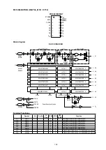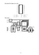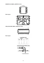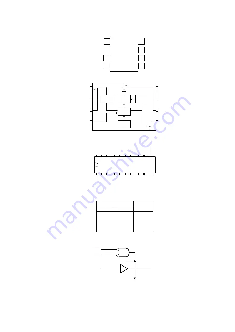
BD82065FVJ-E2 (DIGITAL_NETWORK : IC801)
Block diagram
SN74LVC827APWR (DIGITAL_NETWORK : IC804)
Block diagram
(EXEWLIIX
2013.03.11 Rev.001
63,1'S0XH%PPVMKLXWVIWIVZIH
87>
[[[VSLQGSNT
BD82061FVJ BD82065FVJ
TSZ02201-0E3E0H300350-1-1
9:03
-2
+2(
'LEVKI
4YQT
+EXI
0SKMG
3'(
87(
-2
)2
)2
398
398
398
3'
)2
+2(
-2
-2
398
398
398
3'
)2
+2(
-2
-2
398
398
398
3'
-3
+2(
-2
)2)2
-
0S[
32
&(*:.
,MKL
32
&(*:.
,MKL
":0S[
:
3'
3
0S[
398
3
&(*:.
834:-);
&(*:.
834:-);
www
.ti.com
FEATURES
DB, DGV
, DW
,
N
S
,
O
R
P
W
P
ACKAGE
(T
O
P
V
IE
W
)
1
2
3
4
5
6
7
8
9
10
1
1
12
24
23
22
21
20
19
18
17
16
15
14
13
OE1
A1
A2
A3
A4
A5
A6
A7
A8
A9
A10
GND
V
C
C
Y1
Y2
Y3
Y4
Y5
Y6
Y7
Y8
Y9
Y10
OE2
DESCRIPTION/ORDERING
INFORMATION
SN74LVC827A
10-BIT
BUFFER/DRIVER
WITH
3-STATE
OUTPUTS
SCAS306J
–
MARCH
1993
–
REVISED
FEBRUARY
2005
•
Operates
From
1.65
V
to
3.6
V
•
Inputs
Accept
Voltages
to
5.5
V
•
Max
t
pd
of
6.7
ns
at
3.3
V
•
Typical
V
OLP
(Output
Ground
Bounce)
<0.8
V
at
V
CC
=
3.3
V,
T
A
=
25
°
C
•
Typical
V
OHV
(Output
V
OH
Undershoot)
>2
V
at
V
CC
=
3.3
V,
T
A
=
25
°
C
•
Supports
Mixed-Mode
Signal
Operation
on
All
Ports
(5-V
Input/Output
Voltage
With
3.3-V
V
CC
)
•
I
off
Supports
Partial-Power-Down
Mode
Operation
•
Latch-Up
Performance
Exceeds
250
mA
Per
JESD
17
•
ESD
Protection
Exceeds
JESD
22
–
2000-V
Human-Body
Model
(A114-A)
–
200-V
Machine
Model
(A115-A)
–
1000-V
Charged-Device
Model
(C101)
This
10-bit
buffer/bus
driver
is
designed
for
1.65-V
to
3.6-V
V
CC
operation.
The
SN74LVC827A
provides
a
high-performance
bus
interface
for
wide
data
paths
or
buses
carrying
parity.
The
3-state
control
gate
is
a
2-input
AND
gate
with
active-low
inputs
so
that,
if
either
output-enable
(OE1
or
OE2)
input
is
high,
all
ten
outputs
are
in
the
high-impedance
state.
The
SN74LVC827A
provides
true
data
at
its
outputs.
Inputs
can
be
driven
from
either
3.3-V
or
5-V
devices.
This
feature
allows
the
use
of
this
device
as
a
translator
in
a
mixed
3.3-V/5-V
system
environment.
To
ensure
the
high-impedance
state
during
power
up
or
power
down,
OE
should
be
tied
to
V
CC
through
a
pullup
resistor;
the
minimum
value
of
the
resistor
is
determined
by
the
current-sinking
capability
of
the
driver.
This
device
is
fully
specified
for
partial-power-down
applications
using
I
off
.
The
I
off
circuitry
disables
the
outputs,
preventing
damaging
current
backflow
through
the
device
when
it
is
powered
down.
ORDERING
INFORMATION
T
A
PACKAGE
(1)
ORDERABLE
PART
NUMBER
TOP-SIDE
MARKING
Tube
of
25
SN74LVC827ADW
SOIC
–
DW
LVC827A
Reel
of
2000
SN74LVC827ADWR
SOP
–
NS
Reel
of
2000
SN74LVC827ANSR
LVC827A
SSOP
–
DB
Reel
of
2000
SN74LVC827ADBR
LC827A
–40
°
C
to
85
°
C
Tube
of
60
SN74LVC827APW
TSSOP
–
PW
Reel
of
2000
SN74LVC827APWR
LC827A
Reel
of
250
SN74LVC827APWT
TVSOP
–
DGV
Reel
of
2000
SN74LVC827ADGVR
LC827A
(1)
Package
drawings,
standard
packing
quantities,
thermal
data,
symbolization,
and
PCB
design
guidelines
are
available
at
www.ti.com/sc/package.
Please
be
aware
that
an
important
notice
concerning
availability,
standard
warranty,
and
use
in
critical
applications
of
Texas
Instruments
semiconductor
products
and
disclaimers
thereto
appears
at
the
end
of
this
data
sheet.
PRODUCTION
DATA
information
is
current
as
of
publication
date.
Copyright
©
1993–2005,
Texas
Instruments
Incorporated
Products
conform
to
specifications
per
the
terms
of
the
Texas
Instruments
standard
warranty.
Production
processing
does
not
necessarily
include
testing
of
all
parameters.
www.ti.com
Y1
To Nine Other Channels
OE1
OE2
A1
1
13
2
23
SN74LVC827A
10-BIT BUFFER/DRIVER
WITH 3-STATE OUTPUTS
SCAS306J – MARCH 1993 – REVISED FEBRUARY 2005
FUNCTION TABLE
INPUTS
OUTPUT
Y
OE1
OE2
A
L
L
L
L
L
L
H
H
H
X
X
Z
X
H
X
Z
LOGIC DIAGRAM (POSITIVE LOGIC)
2
141
Содержание AVR-S710W
Страница 8: ...8 Personal notes ...
Страница 144: ...NJU72340AFH3 DIGITAL_ANALOG IC821 NJU72340A Terminal Functions 144 ...
Страница 147: ...2 FL DISPLAY FLD 018BT021GINK FRONT FL101 PIN CONNECTION GRID ASSIGNMENT 147 ...
Страница 148: ...ANODE CONNECTION 148 ...
Страница 168: ...EXPLODED REF No Part No Part Name Remarks Q ty New Ver S14 nsp SCREW CTW3 6JR VTW3 6JR 2 20 ...


