background image


DELTA ELECTRONICS, INC.


12 2008/1/23

Rev. 6G

www.deltaww.com


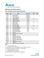
6) 

State/ Control Bits 

Byte 

 Bit 

Name 

Description 

110 

Tx Disable State 

Digital state of the Tx disable input pin 

110 

Soft Tx Disable 

Read/ Write bit that allow software disable of laser 

110 5 

Reserved 


110 

Rate Select tate 

NA 

110 

Soft Rate Select 

NA 

110 

Tx Fault 

Digital state of the Tx fault output pin 

110 1 

LOS 

Digital 

state 

of the LOS output pin. 

110 

Data_Ready_Bar 

NA 

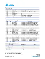
7) 

Optional Set of Alarm and Warning 

Byte 

 Bit 

Name 

Description 

112 

Temp High Alarm 

Set when internal temperature exceeds high alarm level 

112 

Temp Low Alarm 

Set when internal temperature is below low alarm level 

112 

Vcc High Alarm 

Set when internal supply voltage exceeds high alarm level 

112 

Vcc Low Alarm 

Set when internal supply voltage is below low alarm level 

112 

Tx Bias High Alarm 

Set when Tx Bias current exceeds high alarm level 

112 

Tx Bias Low Alarm 

Set when Tx Bias current is below low alarm level 

112 

Tx Power High Alarm 

Set when Tx output power exceeds high alarm level 

112 

Tx Power Low Alarm 

Set when Tx output power is below low alarm level 

113 

Rx Power High Alarm 

Set when received power exceeds high alarm level 

113 

Rx Power Low Alarm 

Set when received power is below low alarm level 

113 

5-0 

Reserved 


116 

Temp High Warning 

Set when internal temperature exceeds high warning level 

116 

Temp Low Warning 

Set when internal temperature is below low warning level 

116 

Vcc High Warning 

Set when internal supply voltage exceeds high warning level 

116 

Vcc Low Warning 

Set when internal supply voltage is below low warning level 

116 

Tx Bias High Warning 

Set when Tx Bias current exceeds high warning level 

116 

Tx Bias Low Warning 

Set when Tx Bias current is below low warning level 

116 

Tx Power High Warning 

Set when Tx output power exceeds high warning level 

116 

Tx Power Low Warning 

Set when Tx output power is below low warning level 

117 

Rx Power High Warning 

Set when received power exceeds high warning level 

117 

Rx Power Low Warning 

Set when received power is below low warning level 

117 

5-0 

Reserved 


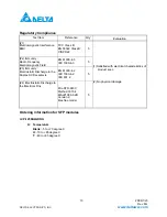
Digital Diagnostic Monitor Accuracy


Parameter 

Typical Value 

Note 

Transceiver Temperature 

±

 3


Power Supply Voltage 

±

 3% 

TX Bias Current 

±

 10% 


TX Optical Power 

±

 1.5dB 


RX Optical Power 

±

 3dB 


Notes: 

1)  Temperature is measured internal to the transceiver. 

2) 

Voltage is measured internal to the transceiver.


Содержание Single Mode SFP Transceiver LCP-1250B4QDRx

Страница 1: ...ressly for high speed communication applications that require rates up to 1 25Gb s The transceiver is data rate transparent which means it can support GbE 1 25Gb s as well as 1x Fiber channel 1 062Gb s operations The LCP 1250B4QDRx series are designed to be compliant with SFP Multi source Agreement MSA Digital diagnostic monitoring functions Temperature VCC TX optical power TX laser bias current a...

Страница 2: ...Input Voltage VDT 0 5 2 4 V 1 Transmitter Disable Input High VDISH 2 VCC 0 3 V Transmitter Disable Input Low VDISL 0 0 8 V Transmitter Fault Pull up Resistor RTX_FAULT 4 7 10 kΩ 2 Transmitter Fault Output High VTXFH 2 VCC 0 3 V 2 Transmitter Fault Output Low VTXFL 0 0 8 V 2 Receiver Receiver Differential Output Voltage VDR 0 35 2 V 3 Receiver LOS Load RRXLOS 4 7 10 kΩ 2 LOS Output Voltage High VLO...

Страница 3: ... 1355 nm Spectral Width RMS σ 4 nm Optical Rise Fall Time tr tf 260 psec 1 Receiver Sensitivity Avg PIN 20 dBm 2 Input Optical Wavelength λ 1270 1570 nm LOS Deasserted Avg PA 19 dBm LOS Asserted Avg PD 36 dBm LOS Hysteresis PA PD 0 5 dB Overload PO 3 dBm Notes 1 These are unfiltered 20 80 values 2 The sensitivity is provided at a BER of 1 10 12 or better with an input signal consisting of 1250Mb s...

Страница 4: ...al ID interface 6 MOD DEF0 Module Definition 0 3 Note 3 Grounded in Module 7 Rate Select Not Connect 3 Function not available 8 LOS Loss of Signal 3 Note 4 9 VeeR Receiver Ground 1 Note 5 10 VeeR Receiver Ground 1 Note 5 11 VeeR Receiver Ground 1 Note 5 12 RD Inv Received Data Out 3 Note 6 13 RD Received Data Out 3 Note 7 14 VeeR Receiver Ground 1 Note 5 15 VccR Receiver Power 2 3 3 5 Note 7 16 Vc...

Страница 5: ...on In the low state the output will be pulled to 0 8V 5 VeeR and VeeT may be internally connected within the SFP module 6 RD These are the differential receiver outputs They are AC coupled 100Ω differential lines which should be terminated with 100Ω differential at the user SERDES The AC coupling is done inside the module and is thus not required on the host board The voltage swing on these lines ...

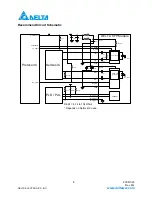
Страница 6: ... 01uF 0 01uF 0 1uF 10uF RES1 RES1 100 Ohms RES1 RES1 RES1 10k Ohms 100 Ohms VCC Protocol Vcc SerDes IC Protocol IC PLD PAL Mod_def 2 Mod_def 1 Mod_def 0 3 3V 3 3V DELTA SFP Module Preamp Tx_Disable Quantizer Tx_Fault TD TD VeeT RD RD Rx_LOS VeeR Tx_Disable Tx_Fault Rx_LOS RES1 4 7k to 10k Ohms VccT VccR Laser Driver Depands on SerDes IC used EEPROM ...

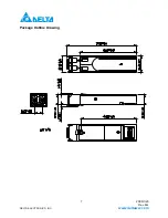
Страница 7: ...DELTA ELECTRONICS INC 7 2008 1 23 Rev 6G www deltaww com Package Outline Drawing ...

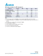
Страница 8: ... 5 LOS Assert Time t_loss_on 100 μsec 6 LOS Deassert Time t_loss_off 100 μsec 7 Serial ID Clock Rate f_serial_clock 100 kHz Notes 1 Time from rising edge of TX_DISABLE to when the optical output falls below 10 of nominal 2 Time from falling edge of TX_DISABLE to when the modulated optical output rises above 90 of nominal 3 From power on or negation of TX_Fault using TX Disable 4 Time from fault to...

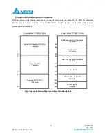
Страница 9: ...about the module s present operating conditions 2 wire address 1010000 X A0h 2 wire address 1010001 X A2h 0 0 55 Alarm and Warning Thresholds 56 bytes 95 Serial ID Defined by SFP MSA 96 bytes 56 95 Cal Constants 40 bytes 96 96 119 Real Time Diagnostic Interface 24 bytes 127 Vender Specific 32 bytes 120 127 Vender Specific 128 128 247 User Writable EEPROM 120 bytes 255 Reserved in SFP MSA 128 bytes...

Страница 10: ...Note 5 106 00 21 45 E 64 00 107 00 22 4C L 65 1A 108 00 23 54 T 66 00 109 00 24 41 A 67 00 110 00 25 20 68 SN Note 6 111 00 26 20 69 SN 112 00 27 20 70 SN 113 00 28 20 71 SN 114 00 29 20 72 SN 115 00 30 20 73 SN 116 00 31 20 74 SN 117 00 32 20 75 SN 118 00 33 20 76 SN 119 00 34 20 77 SN 120 00 35 20 78 SN 121 00 36 00 79 SN 122 00 37 00 80 SN 123 00 38 00 81 SN 124 00 39 00 82 SN 125 00 40 4C L 83...

Страница 11: ...2 TX Power High Warning P 2 30 31 2 TX Power Low Warning P 2 dBm 3 32 33 2 RX Power High Alarm P0 3 34 35 2 RX Power Low Alarm PS 2 36 37 2 RX Power High Warning P0 2 38 39 2 RX Power Low Warning PS dBm 4 40 45 16 Reversed 56 91 36 External Calibration Constants 92 94 3 Reversed 95 1 Checksum 5 96 97 2 Real Time Temperature 98 99 2 Real Time Supply Voltage 100 101 2 Real Time Tx Bias Current 102 1...

Страница 12: ...ow low alarm level 113 7 Rx Power High Alarm Set when received power exceeds high alarm level 113 6 Rx Power Low Alarm Set when received power is below low alarm level 113 5 0 Reserved 116 7 Temp High Warning Set when internal temperature exceeds high warning level 116 6 Temp Low Warning Set when internal temperature is below low warning level 116 5 Vcc High Warning Set when internal supply voltag...

Страница 13: ... 4 3 IEC 1000 4 3 5 3 Immunity Electrostatic Discharge to the Duplex SC Receptacle EN 61000 4 2 IEC 1000 4 2 IEC 801 2 5 4 Electrostatic Discharge to the Electrical Pins MIL STD 883C Method 3015 4 EIAJ 1988 3 2B Version 2 Machine model 5 1 Satisfied with electrical characteristics of product spec 2 No physical damage Ordering information for SFP modules LCP 1250B4QDRX1 X1 Temperature Blank 5 to 70...

Отзывы: