background image

3: Audio/Filter Board

PRC1099A-MS

3-13

3.2.7

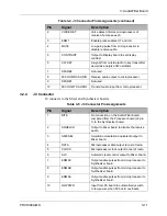
J7 to J12 Coax Connectors

Connector J7 to J12 are RF coax connector carrying either transmit or receive 
or BFO signals as listed below.

3.3

Component Locations, Schematics, and Parts List

This section provides a component location diagram, schematic and parts list 
for the Audio/Filter board.

8

GND

Connects to low side of front panel Volume 
control.

9

600 OHM RX AUDIO

Receive audio output to front panel 
Accessory connector

10

ATU TUNE

Input from Accessory connector to key radio 
and CW oscillator for tuning of external 
equipment.

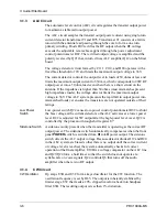
Table 3-7  J6 Connector Pin Assignments (continued)

Pin

Signal

Description

Connector

Signal

J7 - BFO IN

1650 kHz BFO from the Synthesizer board.

J8 - RX OUT

Modulated receive signal (selected channel frequency) output 
to the Mixer board.

J9 - RX IN

Modulated receive signal (1650 kHz) input from the 1650 kHz 
IF board.

J10 - TX OUT

Modulated transmit signal (1650 kHz) output to 1650 kHz IF 
board.

J11 - RF IN

5/20W modulated transmit signal (selected channel frequency) 
input from the PA board.

J12 - RF OUT

Transmit: 5/20W modulated transmit signal (selected channel 
frequency) to the Antenna Tuner board.

Содержание PRC1099A

Страница 1: ...PRC1099A HF Transceiver Technical Manual Manual Part No PRC1099A MS Release Date February 2017 Revision S ...

Страница 2: ...Datron World Communications Inc 995 Joshua Way Suite A Vista CA 92081 U S A Phone 760 597 1500 Fax 760 597 1510 E Mail customerservice dtwc com www dtwc com ...

Страница 3: ... 1 3 6 19 Chapter 6 Chapters 3 4 6 6 11 R Update component locations diagrams schematics and parts lists to the latest revisions Chapter 4 Chapter 6 02 17 S Updated manual format Eliminated Chapter 2 Installation This information is covered in the Operator manual Renamed and restructured Chapters 3 and 4 Divided Chapter 4 into separate chapters for each board Added Front Panel Assembly chapter Upd...

Страница 4: ......

Страница 5: ...re Licensee further agrees they or their agents are not authorized to make derivative versions or changes to the Software Title to and ownership of the Software shall at all times remain with Datron and or its licensors Further no license is granted to copy or reproduce in any form whatsoever the Software supplied without the express written permission of Datron prior to any such contemplated acti...

Страница 6: ...ttempts to repair or modify the equipment Defects or failures caused by Buyer abuse or misuse Return of Equipment Domestic To obtain performance of any obligation under this warranty the equipment must be returned freight prepaid to Technical Support Services Datron World Communications Inc 3055 Enterprise Court Vista California 92081 The equipment must be packed securely Datron shall not be respo...

Страница 7: ...e ground has been established Consult the manual section on grounding Servicing Only trained personnel should perform product repair To avoid electric shock DO NOT open the case unless qualified to do so Various measurements and adjustments described in this manual are performed with AC power applied and the protective covers removed Capacitors particularly the large power supply electrolytic type...

Страница 8: ......

Страница 9: ...4 2 6 DC Power 2 5 Table 2 1 Board Functionality 2 5 2 7 Radio Menu Descriptions 2 11 Table 2 2 Menu Selection 2 11 Figure 2 2 PRC1099A System Block Diagram 2 14 Figure 2 3 PRC1099A Wiring Diagram 994171 Rev C 2 15 Table 2 3 Mainframe Parts List PRC1099ABA Rev T 2 17 Chapter 3 Audio Filter Board 3 1 Circuit Description 3 1 Figure 3 1 Audio Filter Board Block Diagram 3 1 Table 3 1 Audio Filter Boar...

Страница 10: ...t 4 5 Figure 4 2 1650 kHz IF Board Component Locations 738028 Rev D 4 6 Figure 4 3 1650 kHz IF Board Schematic Diagram 994207 Rev B 4 7 Table 4 3 1650 kHz IF Board Parts List 009 00202 Rev R 4 9 Chapter 5 Mixer Board 5 1 Circuit Description 5 1 Figure 5 1 Mixer Board Block Diagram 5 1 Figure 5 2 ALC Frequency vs PA Output Power 5 5 Figure 5 3 AME Option Circuit 5 7 Table 5 1 Mixer Board Specificat...

Страница 11: ...7 10 Figure 7 4 Antenna Tuner Driver Board Schematic Diagram 994303 Rev B 7 11 Table 7 3 Antenna Tuner Driver Board Parts List 009 00502 Rev K 7 13 Table 7 4 Antenna Tuner Board Parts List 009 00503 Rev K 7 16 Chapter 8 Synthesizer Board 8 1 Circuit Description 8 1 Figure 8 1 Synthesizer Board Block Diagram 8 1 Table 8 1 Sample FTW Programming Values 8 4 8 2 Connector Pin Assignments 8 4 Table 8 2...

Страница 12: ...ription 10 1 10 2 Connector Pin Assignments 10 2 Table 10 1 J1 Connector Pin Assignments 10 2 Table 10 2 J2 Connector Pin Assignments 10 4 Table 10 3 J3 Connect Pin Assignments 10 5 Table 10 4 J4 Connect Pin Assignments 10 6 10 3 Component Locations Schematics and Parts List 10 7 Figure 10 1 Display Board Component Location Diagram 738220 Rev G 10 8 Figure 10 2 Display Board Schematic Diagram 9941...

Страница 13: ... 13 2 ALE Signal Connections and Adjustment Points 13 6 Figure 13 3 ALE Board Component Locations 1 of 2 738215 Rev B 13 7 Figure 13 4 ALE Board Component Locations 2 of 2 738215 Rev B 13 8 Figure 13 5 ALE Board Schematic Diagram 994166 Rev G 13 9 Table 13 2 ALE Board Parts List 010 00200 Rev V 13 11 13 2 Internet Protocol Interface PRC1099A IP 13 14 Chapter 14 Maintenance 14 1 Test Equipment 14 1...

Страница 14: ...nections and Adjustment Points 14 24 Table 14 5 1650 kHz IF Board Adjustments 14 25 Figure 14 8 1650 kHz IF Board Adjustment Points 14 25 Table 14 6 Mixer Board Adjustments 14 25 Figure 14 9 Mixer Board Signal Connections and Adjustment Points 14 26 Table 14 7 PA Board Adjustments 14 27 Figure 14 10 PA Board Signal Connections and Adjustment Points 14 27 ...

Страница 15: ...n systems The PRC1099A includes the following features 1 6 to 30 MHz transmit frequency range adjustable in 10 Hz steps Menu driven control from front panel LCD Rugged chassis configurable for manpack mobile and base station systems ALE option This manual provides technical information for the service and repair of the PRC1099A Included are schematic diagrams operational theory test and alignment ...

Страница 16: ...ator LCD battery icon Antenna Port BNC for 50 ohm broadband antennas or for connection to external amplifier whip antenna port Display Multifunction custom LED with backlight Mechanical Environmental Size W x H x D including battery pack 11 1 in x 4 1 in x 9 25 in 28 2 cm x 10 5 cm x 23 5 cm Weight 9 7 lb 4 4 kg without battery pack BB LA6 pack 5 2 lb 2 4 kg Package Olive drab green sealed includi...

Страница 17: ...with an AM receiver BITE Built in test equipment Internal firmware that tests the installed hardware and boards in the radio to verify presence and functionality CW Continuous wave signal Also known as Morse code Channel A group of preset parameters stored in permanent memory associated with a transmit and receive frequency Squelch Audio derived noise immune Audio 500 mW into 16 ohm 50 mW at 150 o...

Страница 18: ... syllabic squelch that reduces background noise to a received signal by turning off the speaker unless audio voice is detected This eliminates the noise between syllables during normal voice audio USB Upper sideband The information carrying band of frequencies above the carrier frequency in SSB transmissions VSWR Voltage standing wave ratio The ratio of peak voltage in the standing wave to the min...

Страница 19: ... 1 6 to 30 MHz The receive signal is first up converted from the selected channel frequency to the 75 MHz IF and then down converted to either 1650 or 1647 kHz IF modulated by the receive audio In transmit mode the PRC1099A mixes the modulated 1650 or 1647 kHz IF with the 73 35 MHz second LO to the first IF output at 75 MHz the Direct Digital Synthesizer DDS generates the first local oscillator LO...

Страница 20: ...ominal life of ten years provides DC power backup for the RAM The serial peripheral interface SPI bus delivers data and control signals to the appropriate boards The data is decoded on the individual boards The front panel controls also interface with the processor to control and configure radio functions The serial data extends to the Accessory connector to control external accessories such as a ...

Страница 21: ...utput is amplified using a high dynamic range amplifier before passing through the 4 pole monolithic 75 MHz filter The 75 MHz filter maintains the 11 dBm intercept point through to the output Output from the 75 MHz filter is amplified by an AGC controlled dual gate MOSFET amplifier and is then down converted in a dual gate MOSFET mixer to the second LO LO2 to 1650 kHz and output to the 1650 kHz IF...

Страница 22: ...ere it is applied to an TX IF amplifier and then filtered with a 6 pole crystal sideband filter where either the upper or lower sideband is removed From the crystal filter the single sideband SSB transmit signal is routed to the Mixer board 2 5 3 Mixer Board Transmit Path From the 1650 kHz IF board the 1650 kHz SSB suppressed carrier transmit signal is applied to the Mixer board where a balanced m...

Страница 23: ...ntenna Tuner board uses detectors at the transmit signal input and follows a tuning routine controlled by the processor to match the radio output impedance to the antenna for maximum output To protect the RF power amplifiers from damage the output is automatically switched to the 50 ohm antenna connector when the whip or long wire antenna is removed 2 6 DC Power The PRC1099A operates from a 12 to ...

Страница 24: ...ilter Switching K2 K11 Decodes serial data selects correct filter range Input serial data from Processor board Output switches RF filters in and out of transmit and receive path ALC Q21 Transmit Measures RF current RF voltage Provides 5W and 20W level output control Input from TX PA output Output to Sidetone Gate ALC gain Mixer board T R Relay K13 Switches TX RX RF and R 8V and T 8V lines Input fr...

Страница 25: ...MHz filter Y1 75 MHz Crystal Filter Y1 Transmit Filters 75 MHz IF signal for transmit path Input from 75 MHz IF amplifier Q11 Output to MX1 mixer Receive Filters 75 MHz IF signal for receive path Input from 75 MHz IF amplifier U4 Output to RX amplifier Q7 RX 75 MHz IF Amp Q7 Receive Amplifies 75 MHz IF RX signal controlled by AGC circuit Input from 75 MHz filter Y1 Input from ALC on 1650 kHz IF Bo...

Страница 26: ...1 Transmit Amplifies 1 6 to 30 MHz transmit signal Inputs transmit signal from 30 MHz LPF Outputs to PA board through J1 A2 Voltage Regulator Q3 Transmit Provides a constant current source to transmit amplifier U1 in transmit mode Inputs 12V from the Junction board Outputs constant 100 mA to U1 Power Amplifier Board Predriver U1 Transmit Class A amplifier amplifies transmit signal to the necessary...

Страница 27: ...h matching network for maximum power transfer Input receive signal at the select channel frequency from either whip antenna or 50 Ohm front panel antenna connector Outputs receive signal at selected channel frequency to low pass filters on the Audio Filter board Serial Decoders and Relay Drivers U2 U3 U4 N A Selects inductors or capacitors to insert into either transmit or receive signal paths for...

Страница 28: ...Inputs 12V from the battery through the front panel jumper on the Accessory connector and the front panel Power switch Outputs 5V supply voltage to the various boards 8V Regulator U2 N A Converts switched 12V to 8V supply voltage Inputs 12V from the battery through the front panel jumper on the Accessory connector and the front panel Power switch Output to 8V supply voltage to the various boards S...

Страница 29: ...nds the radio is to remain at each scanning channel during the scan cycle Scan Hold To select the amount of time the radio is to remain at a particular channel during the scan cycle after a link Voice Detect Select To detect voice communication of scanned channels and stop at those channels when voice communications are detected Voice Detect Hold To set the amount of time the radio remains at that...

Страница 30: ...E is completed the result is displayed on the front panel Frequency Lock To prevent radio channel frequencies from being accidentally changed Once activated the radio channel frequencies cannot be changed until this selection is deactivated Battery Test To check the battery voltage The battery is checked in increments of 0 25 VDC A display of BATT BAD indicates the battery is either below 10 5 or ...

Страница 31: ...ed in an ALE message Message Number To indicate which message if any is to be sent with an ALE transmission The message to send is entered or modified using the selection described in Tx Message If no message is to be sent NONE IS SELECTED Table 2 2 Menu Selection continued Menu Selections Description ...

Страница 32: ... Filter TX Amp RX Path TX Path Oscillator Path Power Amp Power Amplifier Board Processor Control Processor Board Microphone Mixer Board RX Mixer TX Amp 75 MHz Filter RX Amp BAL Mixer Filter RX Amp TX Mixer TX Amp BFO Synthesizer Reference Oscillator Synthesizer Board Audio Filter Board Speaker or Handset First LO 76 6 105 MHz Second LO 73 35 MHz ALC ALC 1650 kHz 1647 kHz Channel Frequency 1 6 to 3...

Страница 33: ...le NONE Rev D Schematic Date Date Appr Drawn Size Drawing Number Sheet 1 of 1 Datron World Communications Inc 3055 Enterprise Ct Vista CA 92081 8362 TEL 760 597 1500 FAX 760 597 1510 HALVERSON REV ECN DESCRIPTION DATE APPR A B C PRC1099 287 RELEASE PRC1099 373 ADD FILTER TX AUDIO 9 21 92 11 9 95 10 20 10 10 0539 SEE ECN ...

Страница 34: ... 214103 CAP 0 01UF X7R 50V 10 0 1LS C7 214103 CAP 0 01UF X7R 50V 10 0 1LS C9 214103 CAP 0 01UF X7R 50V 10 0 1LS L1 459032 IND ASY 3T 30 MAGNET 1 490201 L10 459032 IND ASY 3T 30 MAGNET 1 490201 L2 459032 IND ASY 3T 30 MAGNET 1 490201 L3 459032 IND ASY 3T 30 MAGNET 1 490201 L4 459032 IND ASY 3T 30 MAGNET 1 490201 L5 459032 IND ASY 3T 30 MAGNET 1 490201 L6 459032 IND ASY 3T 30 MAGNET 1 490201 L7 4590...

Страница 35: ......

Страница 36: ...d Modulator VOGAD Sidetone Switch CW Hold Timer Gates Squelch Circuit RX IN J9 BFO IN J7 TX OUT J10 RX OUT J8 High Pass Filter K13 T R Relay from the Power Amplifier board Low Pass Filters Low Power Control 5W 1 6 30 MHz 2 0 2 99999 MHz ALC Detectors Relay Drivers and Serial Decoder Low Power Switch 5W 3 0 4 99999 MHz 20 0 30 0MHz 13 0 19 99999MHz 8 0 12 99999 MHz 5 0 7 99999 MHz SPI DATA SPI CLK ...

Страница 37: ...etermines how fast the compandor reacts to changes in the audio signal Op amp U8D is the output signal amplifier that brings the audio signal to the level required for the balanced modulator The voltage divider network of resistors R126 and R127 set the gain of output signal amplifier U8D Accessory Connector Audio Input Attenuator and RF filter C31 L13 C32 and R46 attenuate and filter the high lev...

Страница 38: ... precision capacitors to remove high frequency noise and harmonics Relay Drivers and Decoder The microprocessor on the Processor board selects the correct low pass filter using latching relays K1 through K12 The latching relays use dual windings and require separate current pulses to open or close the relay Latching relays are only energized to open or close the relay otherwise they are not energi...

Страница 39: ...oard to the 1650 kHz IF board where the unwanted frequencies are filtered out and the 1650 kHz or 1647 kHz IF signal and the signal is amplified The 1650 kHz IF board is discussed in Chapter 4 After the 1650 kHz IF board the modulated IF signal is returned to the Audio Filter board through J9 RX IN where it is applied to the product detector Product Detector Product detector U4 is an integrated ci...

Страница 40: ... after the last syllabic change is detected The squelch is turned off when the timer output is grounded through R18 MUTE The microprocessor can also disable the audio through D23 by setting the output at U9 pin 5 low Squelch Gates Squelch switch PNP bipolar transistor Q6 turns off the receive audio by switching off the 12 V supply to U5 Q6 is controlled by the input from side tone switch Q24 or by...

Страница 41: ...he rapid fall in output power into mismatched loads yet ensures the transistors are not operated outside of their ratings Low Power Switch Low power switch Q22 causes low power control potentiometer R82 to shunt the bias voltage at the current detector so the ALC activates at a lower power level R82 is adjusted for 5W output after the high power level is set Q22 is controlled by the processor thro...

Страница 42: ...e of K13 switches the antenna from the receive signal to the transmit The other pole switches the regulated 8V line to transmit T8 and receive R8 control lines These two control lines provide for transmit receive functions throughout the receiver Contrast Control Differential amplifier U3D and the associated circuitry make up a temperature sensing contrast control for the Display board Variable re...

Страница 43: ...Grounds the receive audio output from product detector U4 through Q5 Q8 pin 11 Normal low Active high Grounds the modulated transmit line from balanced modulator U6 through Q7 Output State Function Table 3 1 Audio Filter Board Specifications Characteristic Specifications Transmit Current 8 VDC at 31 mA 12 VDC at 0 mA see Note 1 below Output 1650 kHz DSB 80 mV PEP Input Microphone or 1000 Hz Receiv...

Страница 44: ...tinued Characteristic Specifications Range Notch 1 Notch 2 2 0 2 99999 MHz 4 2 MHz 6 1 MHz 3 0 4 99999 MHz 6 6 MHz 9 9 MHz 5 0 7 99999 MHz 10 8 MHz 16 35 MHz 8 0 12 99999 MHz 17 2 MHz 27 0 MHz 13 0 19 99999 MHz 27 6 MHz 43 0 MHz 20 0 30 0 MHz 40 5 MHz 60 4 MHz F F F Cutoff Passband Stopband Notch 1 Notch 2 Table 3 2 J1 Connector Pin Assignments Pin Signal Description 1 ENM6C No connection on Audio...

Страница 45: ...in Signal Description Table 3 3 J2 Connector Pin Assignments Pin Signal Description 1 BITE No connection on the Audio Filter board Jumpered from the Processor board to the Synthesizer board J4 pin 1 2 CLOCK Internal processor clock information 3 DATA Internal processor data information 4 PTT Switches the radio to transmit mode 5 8V 8 VDC supply voltage to Processor board 6 R8 8 VDC in receive only...

Страница 46: ...or Pin Assignments continued Pin Signal Description Table 3 5 J4 Connector Pin Assignments Pin Signal Description 1 BITE No connection on the Audio Filter board Jumpered from the Processor board J2 pin 1 to the Synthesizer board 2 SQUELCH Output to Mixer board to disable the receive audio 3 AME SEL Amplitude modulation equivalent output to Mixer board 4 DATA Microprocessor data output to rest of r...

Страница 47: ... supply voltage from Junction board 8 AGC No connection on the Audio Filter board Jumpered from the Processor board J1 pin 10 to the Mixer and Junction board 9 COMP Connects to Audio Filter board J1 pin 5 only 10 ENM5 Connects to Audio Filter board pin 4 only Table 3 7 J6 Connector Pin Assignments Pin Signal Description 1 GND Transmit audio cable shield to ground 2 50 OHM TX AUDIO Transmit audio i...

Страница 48: ...UNE Input from Accessory connector to key radio and CW oscillator for tuning of external equipment Table 3 7 J6 Connector Pin Assignments continued Pin Signal Description Connector Signal J7 BFO IN 1650 kHz BFO from the Synthesizer board J8 RX OUT Modulated receive signal selected channel frequency output to the Mixer board J9 RX IN Modulated receive signal 1650 kHz input from the 1650 kHz IF boar...

Страница 49: ...3 Audio Filter Board 3 14 PRC1099A MS Figure 3 2 Audio Filter Board Component Locations 738221 Rev J ...

Страница 50: ...17 10 R90 100K 8V C116 10 R88 620 R8 D25 D26 R45 10K Q7 2N3565 J10 TX OUT C30 0 01uF R44 2 2K Q15 PN2907A R54 10K R55 47K 8V 8V D9 1N34A T8 R53 220 R52 10K C81 0 01uF D8 Q27 PN2222A R116 10K C139 100 C140 0 1 R112 1K 5V D G S Q26 VN2222LL C95 01 R60 4 7K Q18 2N3565 C94 47 12V D17 1N751 D16 K13A K13C K13B C92 01 8 9 10 U3C LM324 R67 100K C101 0 1 C102 0 1 R72 1 5K C98 015 R66 1 5K C97 015 R65 50K R...

Страница 51: ... 4 5 6 7 8 9 10 J3 614027 VOL HI WIPER 600 OHM RX AUDIO 600 OHM RX AUDIO 50OHM RXAUDIO 600OHM TX AUDIO 600OHM TX AUDIO 5VIN 5VIN 5VIN 50 OHM TXAUDIO 8VIN 8VIN 12VIN 12VIN CW KEY PTT ENM1 DATA DATA CLOCK CLOCK VOICE DET MUTE SQUELCH CONTRAST ALC ALC RF DET AME SEL SPARE2 SPARE1 LOWPWR LOWPWR ENM6A ENM6A ENM6B ENM6B ENM6C ENM6C ENM5 ENM5 COMP COMP AGC AGC BITE BITE ANT SW R8 R8_rtn T8 T8 ATU TUNE 50...

Страница 52: ... 0 01UF X7R 50V 10 0 1LS C11 275104 CAP 0 1UF X7R 50V 10 RAD 0 1S C110 220101 CAP 100PF MICA 500V 5 DM15 C111 220200 CAP 20PF MICA 500V 5 DM15 C112 214103 CAP 0 01UF X7R 50V 10 0 1LS C113 214103 CAP 0 01UF X7R 50V 10 0 1LS C114 214103 CAP 0 01UF X7R 50V 10 0 1LS C115 214103 CAP 0 01UF X7R 50V 10 0 1LS C116 237100 CAP 10UF AL 16V 20 4X5X1 5LS C117 237100 CAP 10UF AL 16V 20 4X5X1 5LS C118 275104 CAP...

Страница 53: ...LS C14 237100 CAP 10UF AL 16V 20 4X5X1 5LS C140 275104 CAP 0 1UF X7R 50V 10 RAD 0 1S C141 021106003 CAP 10UF X7R 10V 10 0805 C142 021105004 CAP 1UF X7R 25V 10 1206 C143 021105004 CAP 1UF X7R 25V 10 1206 C144 DNP NULL PART VACANT PCB LOCATION C145 021105007 CAP 1 0UF 16V X7R 10 0805 C146 022106003 CAP 10UF TA 16V 20 3216 18 C147 021270000 CAP 27PF NP0 100V 5 0805 C148 021474001 CAP 0 47UF X7R 16V 1...

Страница 54: ...1LS C28 214103 CAP 0 01UF X7R 50V 10 0 1LS C29 021105004 CAP 1UF X7R 25V 10 1206 C3 274183 CAP 0 018UF BX 50V 10 BOX 0 2LS C30 021103000 CAP 0 01UF X7R 50V 5 0805 C31 214103 CAP 0 01UF X7R 50V 10 0 1LS C32 214103 CAP 0 01UF X7R 50V 10 0 1LS C33 214103 CAP 0 01UF X7R 50V 10 0 1LS C34 021106003 CAP 10UF X7R 10V 10 0805 C35 214103 CAP 0 01UF X7R 50V 10 0 1LS C36 214103 CAP 0 01UF X7R 50V 10 0 1LS C37...

Страница 55: ...7 220301 CAP 300PF MICA 500V 5 DM15 C58 220201 CAP 200PF MICA 500V 5 DM15 C59 220560 CAP 56PF MICA 500V 5 DM15 C6 275104 CAP 0 1UF X7R 50V 10 RAD 0 1S C60 220331 CAP 330PF MICA 500V 5 DM15 C61 220221 CAP 220PF MICA 500V 5 DM15 C62 220201 CAP 200PF MICA 500V 5 DM15 C63 220121 CAP 120PF MICA 500V 5 DM15 C64 220360 CAP 36PF MICA 500V 5 DM15 C65 220221 CAP 220PF MICA 500V 5 DM15 C66 220121 CAP 120PF M...

Страница 56: ... 0 01UF X7R 50V 10 0 1LS C93 DNP NULL PART VACANT PCB LOCATION C94 237470 CAP 47UF AL 16V 20 6 3X7 RAD C95 214103 CAP 0 01UF X7R 50V 10 0 1LS C96 214103 CAP 0 01UF X7R 50V 10 0 1LS C97 276153 CAP 0 015UF X7R 50V 10 0 2LS C98 276153 CAP 0 015UF X7R 50V 10 0 2LS C99 211102 CAP 1000PF NP0 100V 2 0 1LS D1 320002 DIODE 1N4148 1N4150 DO 35 D11 320003 DIODE GE 1N34A D12 320002 DIODE 1N4148 1N4150 DO 35 D...

Страница 57: ... ENTRY MOLX J2 614027 CONN 10 POS BOTTOM ENTRY MOLX J3 614027 CONN 10 POS BOTTOM ENTRY MOLX J4 610144 HEADER MLX 10PIN 100 J5 610144 HEADER MLX 10PIN 100 J6 610144 HEADER MLX 10PIN 100 J7 610510 CONN SMB PCB JACK F RT AGL TH J8 610510 CONN SMB PCB JACK F RT AGL TH K1 540066 RELAY SPDT 2A LATCH 12V K10 540066 RELAY SPDT 2A LATCH 12V K11 540066 RELAY SPDT 2A LATCH 12V K12 540066 RELAY SPDT 2A LATCH ...

Страница 58: ...ND ASY 3T 30 MAGNET 1 490201 L21 459032 IND ASY 3T 30 MAGNET 1 490201 L22 459032 IND ASY 3T 30 MAGNET 1 490201 L25 430021 IND 22UH FE 140MA 10 IM 2 L26 045000000 BEAD FERRITE Z 600 0 2A 25 0805 L3 459143 IND ASSY 19T 26 AWG L4 459411 IND ASSY 10T 24GA 2 490033 L5 459117 IND ASSY 15T 24GA 1 490033 L6 459016 IND ASSY 13T 24 GA 1 490034 L7 459059 IND ASSY 12T 24GA 1 490034 L8 459001 IND ASSY 6T 22AWG...

Страница 59: ...OR NPN PN2222A TO92 Q5 310006 XSTR PN3565 NPN 50MA TO 92 Q6 310052 XSTR PN2907A PNP TO92 Q7 310006 XSTR PN3565 NPN 50MA TO 92 Q8 310003 XSTR 2N3567 NPN 300MA TO92 Q9 310003 XSTR 2N3567 NPN 300MA TO92 R1 113335 RES 3 3M OHM 1 8W CF 5 R10 113335 RES 3 3M OHM 1 8W CF 5 R100 113101 RES 100 OHM 1 8W CF 5 R101 113273 RES 27K OHM 1 8W CF 5 R102 113273 RES 27K OHM 1 8W CF 5 R103 113683 RES 68K 1 8W 5 CARB...

Страница 60: ...0 RES 15K OHM 1 8W 1 TK 0805 R127 013110200 RES 11K OHM 1 8W 1 TK 0805 R128 013768100 RES 7 68K OHM 1 8W 1 TK 0805 R129 013472000 RES 4 7K OHM 1 8W 5 TK 0805 R13 113103 RES 10K OHM 1 8W CF 5 R130 013472000 RES 4 7K OHM 1 8W 5 TK 0805 R131 013105000 RES 1M OHM 1 8W 5 TK 0805 R132 013103001 RES 10K OHM 1 8W 1 TK 0805 R133 013303000 RES 30 1K OHM 1 8W 1 TK 0805 R134 013619100 RES 6 19K OHM 1 8W 1 TK ...

Страница 61: ...F 5 R32 113562 RES 5 6K OHM 1 8W CF 5 R33 113103 RES 10K OHM 1 8W CF 5 R34 113272 RES 2 7K OHM 1 8W CF 5 R35 113332 RES 3 3K OHM 1 8W CF 5 R36 012698001 RES 698 OHM 0 1W 1 TK 0603 R37 012330201 RES 33K OHM 1 10W 1 TK 0603 R38 113100 RES 10 OHM 1 8W 5 FILM R39 113153 RES 15K OHM 1 8W CF 5 R4 113473 RES 47K OHM 1 8W CF 5 R40 113682 RES 6 8K 1 8W 5 CARBON FILM R41 012806001 RES 806 OHM 0 1W 1 TK 0603...

Страница 62: ...W CF 5 R63 113103 RES 10K OHM 1 8W CF 5 R64 113103 RES 10K OHM 1 8W CF 5 R65 170232 RES 50K SEALED TRIM 1 4 SQ R66 113152 RES 1 5K OHM 1 8W CF 5 R67 113104 RES 100K OHM 1 8W CF 5 R68 113104 RES 100K OHM 1 8W CF 5 R69 113104 RES 100K OHM 1 8W CF 5 R7 113104 RES 100K OHM 1 8W CF 5 R70 113222 RES 2 2K OHM 1 8W CF 5 R71 113202 RES 2K 1 8W 5 CARBON FILM R72 113152 RES 1 5K OHM 1 8W CF 5 R73 113473 RES ...

Страница 63: ...7K OHM 1 8W CF 5 R93 113103 RES 10K OHM 1 8W CF 5 R94 013124000 RES 120K OHM 1 8W 5 TK 0805 R95 113103 RES 10K OHM 1 8W CF 5 R96 113104 RES 100K OHM 1 8W CF 5 R97 113106 RES 10M 1 8W 5 CARBON FILM R98 113473 RES 47K OHM 1 8W CF 5 R99 113333 RES 33K OHM 1 8W CF 5 T1 459100 IND ASSY 10T 26GA 1 490302 TP1 653003 PIN PRINTED CIRCUIT BOARD U1 330030 IC LIN LM324N DIP14 OP AMP U10 330081 IC LM2904 OP AM...

Страница 64: ...6 XU1 621005 SOCKET IC DIP 14 PIN XU10 621003 SOCKET IC DIP 8 PIN XU2 621005 SOCKET IC DIP 14 PIN XU3 621005 SOCKET IC DIP 14 PIN XU4 621003 SOCKET IC DIP 8 PIN XU5 621003 SOCKET IC DIP 8 PIN XU9 621004 SOCKET IC DIP 16 PIN Table 3 8 Audio Filter Board Parts List 009 00101 Rev AK Designator Part Number Description ...

Страница 65: ......

Страница 66: ... TX Amplifier Transmit IF amplifier Q3 amplifies the low level dual sideband signal from the balanced modulator on the Audio Filter board It also provides correct matching to the 1650 kHz sideband filter 1650 kHz Crystal Sideband Filter The 1650 kHz crystal sideband filter consists of six crystal filters In transmit mode the 1650 kHz sideband filter removes one of the sidebands from the double sid...

Страница 67: ...the BFO by 3 kHz when switching sidebands RX IF Amplifier 1 From the 1650 kHz sideband filter the receive signal is applied to first 1650 kHz IF amplifier Q1 Dual gate MOSFET Q1 amplifies the receive signal from the 1650 kHz sideband filter and integrates the AGC signal to prevent high receive signal levels that may damage components It is capacitor coupled to the filter the amplifier input and ha...

Страница 68: ... The low impedance output drives the base of Q4 through voltage doubler rectifier D3 and D4 DC Amplifier AGC DC amplifier Q4 is a common emitter bipolar transistor with R18 as the high impedance collector load This gives a negative going AGC output of 4V to 0V The AGC output controls the first 1650 kHz IF amplifier Q1 and 75 MHz IF amplifier Q7 on the Mixer board 4 1 4 Specifications Note These sp...

Страница 69: ...utput signal to the Mixer board and the receive input signal from the Mixer board 4 2 4 J4 Connector Coax connector J4 RX OUT carries the receive signal to the Audio Filter board Table 4 2 J1 Connector Pin Assignments Pin Description Connection 1 AGC Automatic gain control for setting the audio level in receive mode to the Mixer board Typically 4 VDC 2 R8 8 VDC when radio is in receive mode 0 VDC ...

Страница 70: ...4 1650 kHz IF Board PRC1099A MS 4 5 4 3 Component Locations Schematics and Parts List This section provides a component location diagram schematic and parts list for the 1650 kHz IF board ...

Страница 71: ...4 1650 kHz IF Board 4 6 PRC1099A MS Figure 4 2 1650 kHz IF Board Component Locations 738028 Rev D ...

Страница 72: ...LE C8 01 J2 TX IN C5 100pF Q1 3N187 R1 15K R2 220 D1 D2 D5 C10 01 L4 R3 220 R6 100K C13 4 7 C12 0 1 C6 01 D7 C23 10 C22 01 R24 2 2K R8 R4 27K C11 0 1 R5 22 T3 C7 01 Q2 2N5770 R20 220 Q4 2N3565 C19 01 D3 D4 C20 01 R22 2 2K Q5 2N3565 R21 100K R23 100K C21 01 C14 01 T4 C15 0 1 R12 22 L3 3T R7 33K R8 3 9K R9 68 C16 0 1 R11 47 R10 47 J4 RX OUT T8 8V AGC 1650 KHz SIDEBAND FILTER RX IF AMP RX IF AMP AGC ...

Страница 73: ... 1LS C20 214103 CAP 0 01UF X7R 50V 10 0 1LS C21 214103 CAP 0 01UF X7R 50V 10 0 1LS C22 214103 CAP 0 01UF X7R 50V 10 0 1LS C23 237100 CAP 10UF AL 16V 20 4X5X1 5LS C25 021104 CAP 0 1UF X7R 50V 10 1206 C3 2751001 CAP 10PF NPO 50V 5 RAD 0 1S C5 221101 CAP 100PF MICA 300V 5 DM5 C6 214103 CAP 0 01UF X7R 50V 10 0 1LS C7 214103 CAP 0 01UF X7R 50V 10 0 1LS C8 214103 CAP 0 01UF X7R 50V 10 0 1LS C9 275104 CA...

Страница 74: ...ES 47 OHM 1 8W 5 CARBON FILM R12 113220 RES 22 OHM 1 8W 5 CARBON FILM R13 113272 RES 2 7K OHM 1 8W CF 5 R14 113153 RES 15K OHM 1 8W CF 5 R15 113101 RES 100 OHM 1 8W CF 5 R16 113104 RES 100K OHM 1 8W CF 5 R17 1110000 RES 0 OHM 1 8W 1 R18 113104 RES 100K OHM 1 8W CF 5 R19 1110000 RES 0 OHM 1 8W 1 R2 113221 RES 220 OHM 1 8W 5 CF R20 113221 RES 220 OHM 1 8W 5 CF R21 113104 RES 100K OHM 1 8W CF 5 R22 1...

Страница 75: ...INDUCTOR IF 1650KHZ T2 420018 INDUCTOR IF 1650KHZ T3 420018 INDUCTOR IF 1650KHZ T4 420018 INDUCTOR IF 1650KHZ Y1 361001 CRYSTAL FILTER TW100 Y2 361004 CRYSTAL FILTER TW100 Y3 361003 CRYSTAL FILTER TW100 Y4 361002 CRYSTAL FILTER TW100 Y5 361001 CRYSTAL FILTER TW100 Y6 361004 CRYSTAL FILTER TW100 Table 4 3 1650 kHz IF Board Parts List 009 00202 Rev R Designator Part Number Description ...

Страница 76: ......

Страница 77: ...ctions discuss the components of the block diagram shown in Figure 5 1 below Figure 5 1 Mixer Board Block Diagram to Power Amplifier Board AGC from Audio Filter Board RX TX ALC SYN 2 73 35 MHz Receive signal to 1650 kHz IF Board 12V SYN 1 76 6 105 MHz 1 Hz Steps TX RX Double Balanced Mixer Current Regulator Squelch Squelch Gate RX Mixer 75 MHz 1650 MHz 30 MHz LO Pass Filter 75 MHz 4 Pole XTAL Filt...

Страница 78: ...gnal at gate 1 pin 4 The ALC signal received from Audio Filter board is applied to ALC amplifier Q12 refer to ALC Circuit on page 3 6 When the ALC circuit is not active a maximum voltage of 4V is applied to gate 2 through voltage divider R54 and R55 The drain of Q11 is connected through broadband transformer T4 to the 50 ohm input of the 75 MHz filter through PIN diode switch D11 D11 is forward bi...

Страница 79: ...ed on by TX gate Q5 that is controlled by the R8 line Transmit Receive Switch The transmit signal is output to the PA board through the transmit receive T R switch controlled by relay K1 The relay is activated by T8 8V The transmit signal is output at the TX OUT terminal 5 1 2 Receive Mode In receive mode the Mixer board receives the receive signal from the Audio Filter board on the RX IN terminal...

Страница 80: ... Crystal Filter 75 MHz filter Y1 is a monolithic 4 pole crystal filter with 25 MHz bandwidth that provides the primary selectivity The filter has a stopband of 70 dB and rejects the IF image and other spurious frequencies The filter output is impedance matched to 50 ohms by the matching network C44 L14 and C45 75 MHz IF Amplifier 2 Dual gate MOSFET Q7 integrates the AGC signal with the filtered 75...

Страница 81: ...signal of 20W from the RF power amplifiers on the PA board in lowest output channels typically the higher frequency channels around 30 MHz The ALC circuit monitors the RF output power on the Audio Filter board to maintain the 20W output in channels where the transmit signal may exceed 20W typically the lower frequency channels around 2 MHz If the output exceeds 20W by a preset value the ALC circui...

Страница 82: ...tion The AME option circuit injects the 1647 or 1650 kHz BFO full carrier signal from the Synthesizer board directly into the transmit path at double balanced mixer U2 as shown in Figure 5 3 on page 5 7 to prevent the carrier being controlled by the ALC circuit The BFO signal is applied to the input of mixer U2 using PIN diode attenuators D14 and D15 as an on off switch In the AME off position D14...

Страница 83: ...U9 DATA from Processor D13 C71 T8 R46 R8 C25 CRYSTAL FILTER 1650 kHz IF Board BALANCED MODULATOR Audio Filter Board Audio Filter Board 2nd LO TX AUDIO IN Low AME Off High AME On 1650 KHZ 1650 kHz BFO T8 Carrier Suppressed Sideband Suppressed 1650 kHz BFO from Synthesizer Table 5 1 Mixer Board Specifications Characteristic Specification Transmit Current 8 VDC at 43 mA 12 VDC at 44 mA Output Channel...

Страница 84: ...Vrms at 73 35 MHz Table 5 1 Mixer Board Specifications continued Characteristic Specification Table 5 2 J1 Connector Pin Assignments Pin Signal Description 1 GND Chassis ground 2 ALC Automatic level control from the Audio Filter board for setting the output power level in transmit mode 3 12V 12 VDC from the Junction board 4 8V 8 VDC from the Junction board 5 R8 8 VDC in receive from Audio Filter b...

Страница 85: ... Receive output to and transmit input from the Audio Filter board A2 TX OUT Transmit output signal to the PA board A3 RX IN Receive input signal from the Audio Filter board Table 5 2 J1 Connector Pin Assignments continued Pin Signal Description Table 5 3 Coax Cable Connections Connector Signal Description J2 LO1 Local oscillator 1 output 76 6 to 105 MHz to the Mixer board J3 LO2 Local oscillator 2...

Страница 86: ...5 Mixer Board 5 10 PRC1099A MS Figure 5 4 Mixer Board Component Locations 738217 Rev H ...

Страница 87: ... 21 92 B PRC1099 291 C1 WAS 01 11 17 92 BS C PRC1099 333 ADD L35 L36 DEL C15 5 31 94 D PRC1099 359 ADD L37 L40 12 21 94 E PRC1099 362 SEE ECN 5 17 95 BS F PRC1099 383 REVISED BIAS CKT JC G ECO 01 0656 ADDED AME OPTION BORDER 12 19 01 JC H ECO 03 0174 ADDED C86 7 23 03 BB J ECO 05 0089 CHG VALUE OF R60 R63 4 21 05 BB K ECO 05 0125 DNP R62 63 ADD R65 5 19 05 BB L ECO 05 0191 ADDED PROTECTION DIODES ...

Страница 88: ... 12V R60 68 ohm R61 51 ohm R65 270 ohm G D S Q5 VN2222LL R17 10 K GND GND R8F GND DNP R13 GND GND GND GND GND GND L12 22uH R20 220 ohm MAR 8 1 2 3 4 U1 GND GND GND GND GND GND D3 R16 2 2K R58 2 2K R6 2 2K D17 BA482 D1 BA482 D2 BA482 R8F L9 L10 T8F GND R15 6 8K L6 R8 100ohm T8F GND GND R8F GND L5 YEL C24 5 5 35pf C17 50pF C18 5pF Y1 75MHZ GND GND C33 0 01u C79 0 1uF 12V GND GND C34 0 01u C35 0 01u ...

Страница 89: ...GND 2 3 4 1 T4 3 4 2 1 Q8 BF998 3 4 2 1 Q7 BF998 3 3 4 4 2 2 1 1 Q11 BF998 GND R23 4 7K GND R8 C52 7PF R26 330K GND GND GND GND R8 GND GND GND GND GND GND GND GND L9 GND SYNTH 2 GND L9 R29 3 3K L20 GND 8V C60 001uF GND GND GND GND R32 100K R36 100K R54 33K R55 100K GND T8 GND GND GND GND L22 C64 15pF GND GND T8 GND C74 22MF GND T8 GND GND R56 150K GND R8 GND 14 CAR 8 ADJ 2 SIG 4 BIAS 5 GAIN 3 OUT ...

Страница 90: ...214103 CAP 0 01UF X7R 50V 10 0 1LS C23 214103 CAP 0 01UF X7R 50V 10 0 1LS C24 261250 CAP 30PF 5MM TRIMMER C25 214103 CAP 0 01UF X7R 50V 10 0 1LS C27 214103 CAP 0 01UF X7R 50V 10 0 1LS C28 275104 CAP 0 1UF X7R 50V 10 RAD 0 1S C29 275104 CAP 0 1UF X7R 50V 10 RAD 0 1S C3 214103 CAP 0 01UF X7R 50V 10 0 1LS C30 275104 CAP 0 1UF X7R 50V 10 RAD 0 1S C31 275104 CAP 0 1UF X7R 50V 10 RAD 0 1S C33 214103 CAP...

Страница 91: ...57 214103 CAP 0 01UF X7R 50V 10 0 1LS C58 261250 CAP 30PF 5MM TRIMMER C59 214103 CAP 0 01UF X7R 50V 10 0 1LS C6 221330 CAP 33PF DM5 300V 5 MICA C60 276102 CAP 1000PF X7R 50V 10 0 1LS C61 214103 CAP 0 01UF X7R 50V 10 0 1LS C62 214103 CAP 0 01UF X7R 50V 10 0 1LS C63 214103 CAP 0 01UF X7R 50V 10 0 1LS C64 210150 CAP 15PF NP0 50V 5 0 1LS DSK C65 261250 CAP 30PF 5MM TRIMMER C66 214103 CAP 0 01UF X7R 50...

Страница 92: ...LS C87 021104000 CAP 0 1UF X7R 25V 5 0805 C9 221101 CAP 100PF MICA 300V 5 DM5 D1 320005 DIODE BA482 PIN SWITCH DO 34 D11 320005 DIODE BA482 PIN SWITCH DO 34 D12 320002 DIODE 1N4148 1N4150 DO 35 D13 320005 DIODE BA482 PIN SWITCH DO 34 D14 DNP NULL PART VACANT PCB LOCATION D15 DNP NULL PART VACANT PCB LOCATION D16 320002 DIODE 1N4148 1N4150 DO 35 D17 320005 DIODE BA482 PIN SWITCH DO 34 D18 037700008...

Страница 93: ...E Z 600 0 2A 25 0805 L27 045000001 BEAD FERRITE Z 120 0 4A 25 1206 L28 045000001 BEAD FERRITE Z 120 0 4A 25 1206 L29 045000001 BEAD FERRITE Z 120 0 4A 25 1206 L3 459031 IND ASSY 16T 26 GA 1 490032 L30 045000001 BEAD FERRITE Z 120 0 4A 25 1206 L31 045000000 BEAD FERRITE Z 600 0 2A 25 0805 L32 045000001 BEAD FERRITE Z 120 0 4A 25 1206 L33 045000001 BEAD FERRITE Z 120 0 4A 25 1206 L34 045000001 BEAD ...

Страница 94: ...82 RES 6 8K 1 8W 5 CARBON FILM R16 113222 RES 2 2K OHM 1 8W CF 5 R17 113103 RES 10K OHM 1 8W CF 5 R18 113153 RES 15K OHM 1 8W CF 5 R2 113153 RES 15K OHM 1 8W CF 5 R20 113221 RES 220 OHM 1 8W 5 CF R21 113103 RES 10K OHM 1 8W CF 5 R22 113103 RES 10K OHM 1 8W CF 5 R23 113472 RES 4 7K OHM 1 8W CF 5 R24 113221 RES 220 OHM 1 8W 5 CF R25 113102 RES 1K OHM 1 8W CF 5 R26 113334 RES 330K OHM 1 8W 5 CF R27 1...

Страница 95: ...PART VACANT PCB LOCATION R48 DNP NULL PART VACANT PCB LOCATION R49 DNP NULL PART VACANT PCB LOCATION R5 113470 RES 47 OHM 1 8W 5 CARBON FILM R50 DNP NULL PART VACANT PCB LOCATION R51 DNP NULL PART VACANT PCB LOCATION R52 DNP NULL PART VACANT PCB LOCATION R53 DNP NULL PART VACANT PCB LOCATION R54 113333 RES 33K OHM 1 8W CF 5 R55 113104 RES 100K OHM 1 8W CF 5 R56 113154 RES 150K OHM 1 8W CF 5 R57 11...

Страница 96: ...T 30 MAG 1 491301 T3 420018 INDUCTOR IF 1650KHZ T4 459034 IND ASSY 1T3T 30 MAG 1 491301 U1 380010 IC MAR 8 RF AMPLIFIER MICRO X U2 330006 IC MC1496P BAL DE MOD DIP14 U3 330343 IC LM317LZ ADJ VREG 100 MA TO 92 U4 033306042 IC BL051 RF AMP 4GHZ SOT89 XY1 868000 GASKET EMI 125 X 0 156 Y1 370007 CRYSTAL FILTER 75MHZ 4 POLE Table 5 4 Mixer Board Parts List 009 00301 Rev AU Designator Part Number Descri...

Страница 97: ......

Страница 98: ...mize current drain The following sections discuss the components of the block diagram in Figure 6 1 below Figure 6 1 Power Amplifier Board Block Diagram 50 ohm 1 6 to 30 MHz 3 dBm 50 ohm 1 6 to 30 MHz 20W Drivers Push Pull Q5 Q2 Q3 Pre Driver TX1 TX1 G ET4 ET5 Final Amplifiers Push Pull PRE REG DT SENS DBIAS U1 T8 PRE REG U2 REG U3 DBIAS PRE REG DT SENS Q6 U4 FBIAS PRE REG FT SENS Q7 T1 T2 T3 FBIA...

Страница 99: ...l Amplifier The final RF amplifier stage consists of RF power amplifiers Q4 and Q5 in a push pull configuration The RF power amplifier transistors are designed for SSB service in the HF range The input from the driver amplifiers is coupled through T2 The transistors operate in class AB using collector to base feedback R16 C20 and R13 C23 The transistor bias is derived from the bias regulator circu...

Страница 100: ...tors change resistance with temperature this means that as the thermistor temperature increases its resistance increases Bipolar transistor Q8 forms a voltage divider with TH1 and conducts when the heat sink temperature exceeds 80 C pulling the LOW POWER line to ground This forces the radio RF power output to 5W or less until the RF power amplifiers cools TH1 is mounted in a hole in the board heat...

Страница 101: ...r Pin Assignments Pin Signal Description 1 12V 12 VDC supply voltage from the Junction board 2 12V 12 VDC supply voltage from the Junction board 3 LOW POWER Line transitions low 0V when the final amplifiers overheat otherwise 5V This sets the radio to low power 5W mode 4 T8 8 VDC supply voltage when radio is in transmit 0 VDC in receive 5 GND Chassis ground 6 GND Chassis ground ...

Страница 102: ...6 Power Amplifier Board PRC1099A MS 6 5 6 3 Component Locations Schematics and Parts List This section provides a component location diagram schematic and parts list for the Power Amplifier board ...

Страница 103: ...6 Power Amplifier Board 6 6 PRC1099A MS Figure 6 2 Power Amplifier Board Component Locations 738617 Rev C ...

Страница 104: ... 0 01UF C52 0 01UF C53 0 01UF C25 0 1UF C18 1000PF C19 1000PF C21 1000PF C22 1000PF C10 0 1UF C14 0 1UF C20 0 1UF C23 0 1UF C27 0 1UF C28 0 1UF Q8 MMBT4401 R17 100 R18 100 R46 10K R47 10K C37 1uF C38 1uF C39 1uF C40 1uF C41 1uF C42 1uF C46 1uF C47 1uF R25 1K R26 1K R27 1K R28 1K R29 1K R30 1K R31 1K R32 1K R33 1K R34 1K R52 1K R53 1K R54 1K R55 1K R56 1K R57 1K D1 1N4005 D2 1N4005 T3 T1 T2 TH1 150...

Страница 105: ...2007 CAP 1000PF NP0 200V 5 1206 C2 021104006 CAP 0 1UF X7R 25V 10 0603 C20 021104011 CAP 0 1UF X7R 100V 10 1206 C21 021102007 CAP 1000PF NP0 200V 5 1206 C22 021102007 CAP 1000PF NP0 200V 5 1206 C23 021104011 CAP 0 1UF X7R 100V 10 1206 C25 021104000 CAP 0 1UF X7R 25V 5 0805 C26 022226003 CAP 22UF TA L ESR 35V 10 7343 C27 021104011 CAP 0 1UF X7R 100V 10 1206 C28 021104011 CAP 0 1UF X7R 100V 10 1206 ...

Страница 106: ...103001 CAP 0 01UF 50V X7R 10 0603 C53 021103001 CAP 0 01UF 50V X7R 10 0603 C54 021225004 CAP 2 2UF X7R 10V 10 0603 C55 021225004 CAP 2 2UF X7R 10V 10 0603 C56 021106003 CAP 10UF X7R 10V 10 0805 C57 021106003 CAP 10UF X7R 10V 10 0805 C59 021102000 CAP 1000PF NP0 100V 5 0805 C6 022226003 CAP 22UF TA L ESR 35V 10 7343 C60 DNP NULL PART VACANT PCB LOCATION C7 021104006 CAP 0 1UF X7R 25V 10 0603 C8 021...

Страница 107: ...10100000 POT 100 OHM 5 T TOP ADJ 4MM R25 012100101 RES 1K OHM 0 1W 1 TK 0603 R26 012100101 RES 1K OHM 0 1W 1 TK 0603 R27 012100101 RES 1K OHM 0 1W 1 TK 0603 R28 012100101 RES 1K OHM 0 1W 1 TK 0603 R29 012100101 RES 1K OHM 0 1W 1 TK 0603 R30 012100101 RES 1K OHM 0 1W 1 TK 0603 R31 012100101 RES 1K OHM 0 1W 1 TK 0603 R32 012100101 RES 1K OHM 0 1W 1 TK 0603 R33 012100101 RES 1K OHM 0 1W 1 TK 0603 R34...

Страница 108: ...10W 1 TK 0603 R6 013560801 RES 5 6 OHM 1 4W 1 TK 1206 R60 013270000 RES 27 OHM 1 8W 5 TK 0805 R61 013270000 RES 27 OHM 1 8W 5 TK 0805 R62 013360900 RES 36 OHM 1 8W 1 TK 0805 R63 014220900 RES 22 OHM 1 4W 1 TK 1206 R64 013470900 RES 47 OHM 1 8W 1 TK 0805 R7 014137000 RES 137 OHM 1 4W 1 TK 1206 R7A DNP NULL PART VACANT PCB LOCATION R8 013560801 RES 5 6 OHM 1 4W 1 TK 1206 R9 013560801 RES 5 6 OHM 1 4...

Страница 109: ... approximately 24 MHz This means that over most of the frequency range the antenna has a capacitive reactance that can be cancelled by an equivalent series inductance The tuner uses a binary sequenced series of inductors to cancel out the reactive component of the antenna If the antenna has inductive reactance the tuner adds capacitance so the antenna appears capacitive and cancels small residual ...

Страница 110: ...o use The transmitter is keyed in low power and the firmware steps through the inductors in a special sequence until it detects a current peak If the tuning program does not detect a current peak the antenna is inductive and the tuning program combines capacitors with the inductors until it detects a tuning peak At this point the tuning program checks the antenna current If the current is low it c...

Страница 111: ... power is automatically reduced when inductors L8 L9 and L10 are in circuit This keeps the maximum output voltage from exceeding approximately 1000V 7 1 6 Shunt Capacitors The tuning program uses shunt capacitors C1 and C2 when the antenna exhibits inductive reactance These capacitors give 50 to 150 pF in 50 pF steps The tuner uses the minimum step size that causes the antenna to appear capacitive...

Страница 112: ...he transformer provides a match of 2 1 or better over the impedance range of 6 ohms to 400 ohms 7 1 10 10 dB Attenuator Relay K15 switches attenuator pad R1 R2 and R3 9 5 dB into the tuning circuit during a tuning cycle The transmitter operates in low power mode 5W during the tune cycle the attenuator further reduces the output power to 500 mW The resistive pad ensures that the transmitter has a t...

Страница 113: ...rs U5 and U6 are 16 NPN transistors contained in two 16 pin DIP packages There are 14 latching relays in the tuner that have separate coils for latching and unlatching the relay The relays require short current pulses for latching or unlatching and draw no current in the static condition Separate drivers latch each relay while transistor Q1 driven by output Q8 of U3A unlatches all relays The proce...

Страница 114: ...at 12V 16 mA average at 5V Rated Input Power Output 1 kV 20W PEP Output exceed 1 kV 5W PEP power level automatically switched by Processor board Maximum Output Voltage 1000V RF Usable Antennas Manual Tune Time 1 sec typical 12 sec maximum before fault Memory Tune Time 20 ms typical Tune Indicator 900 Hz side tone Fault Indicator Pulsating tone Antenna Range 3m whip 2 0 to 30 MHz 7m whip 1 6 to 30 ...

Страница 115: ...he ANT SW signal activates relays K15 and K16 to switch the receive signal between the whip antenna path and the 50 ohm connector path 7 2 2 Transmit Path The transmit path through the Antenna Tuner board is exactly the opposite of the receive path The transmit path is received at onboard connector J3 from the Audio Filter board and is switched to either the whip antenna connector or the 50 ohm co...

Страница 116: ...rts list for the Antenna Tuner board 5 5V 5 VDC supply voltage from the Junction board 6 STROBE Strobes to shift registers from the Processor board 7 COMP OUT Comparator output to the Processor board for tuning cycles 8 ANT SW Antenna switch 0 VDC without antenna 4 8 VDC with 9 10 No connection Table 7 2 J1 Connector Pin Assignments Pin Signal Description ...

Страница 117: ...7 Antenna Tuner Board PRC1099A MS 7 9 Figure 7 2 Antenna Tuner Driver Board Component Locations 738346 Rev B ...

Страница 118: ...7 Antenna Tuner Board 7 10 PRC1099A MS Figure 7 3 Antenna Tuner Board Component Locations 738027 Rev D ...

Страница 119: ...27 01 C28 01 C29 01 C30 01 C31 01 C32 01 R19 2 2K R18 2 2K Q4 2N6427 Q1 2N6039 12 D4 1N4001 D5 12 R12 3 3M R13 1 6M R14 825K R15 402K R16 200K R17 100K C5 100P 1 2 3 U1A LM324 7 6 5 U1B LM324 8 9 10 U1C LM324 14 13 12 U1D LM324 11 4 U1E LM324 12 R11 3 3K R20 2 2K R10 10K R9 10K C2 01 C1 01 Q2 2N3567 Q3 2N3567 R21 100K R7 33K R8 68K R30 820K R5 10K R6 200K C16 2 2 C15 0 1 L1 C14 10 12 C7 47 E1 E2 E...

Страница 120: ... 1LS C2 214103 CAP 0 01UF X7R 50V 10 0 1LS C20 214103 CAP 0 01UF X7R 50V 10 0 1LS C21 214103 CAP 0 01UF X7R 50V 10 0 1LS C22 214103 CAP 0 01UF X7R 50V 10 0 1LS C23 214103 CAP 0 01UF X7R 50V 10 0 1LS C24 214103 CAP 0 01UF X7R 50V 10 0 1LS C25 214103 CAP 0 01UF X7R 50V 10 0 1LS C26 214103 CAP 0 01UF X7R 50V 10 0 1LS C27 214103 CAP 0 01UF X7R 50V 10 0 1LS C28 214103 CAP 0 01UF X7R 50V 10 0 1LS C29 21...

Страница 121: ... R19 124222 RES 2 2K OHM 1 4W 5 CF R20 113222 RES 2 2K OHM 1 8W CF 5 R21 113104 RES 100K OHM 1 8W CF 5 R22 113101 RES 100 OHM 1 8W CF 5 R23 113101 RES 100 OHM 1 8W CF 5 R24 113101 RES 100 OHM 1 8W CF 5 R30 113824 RES 820K OHM 1 8W CF 5 R5 113103 RES 10K OHM 1 8W CF 5 R6 1112003 RES 200K 1 8W 1 FILM R7 113333 RES 33K OHM 1 8W CF 5 R8 113683 RES 68K 1 8W 5 CARBON FILM R9 113103 RES 10K OHM 1 8W CF 5...

Страница 122: ...14 PIN XU2 621004 SOCKET IC DIP 16 PIN XU3 621004 SOCKET IC DIP 16 PIN XU4 621004 SOCKET IC DIP 16 PIN XU5 621004 SOCKET IC DIP 16 PIN XU6 621004 SOCKET IC DIP 16 PIN Table 7 3 Antenna Tuner Driver Board Parts List 009 00502 Rev K Designator Part Number Description ...

Страница 123: ...TCH 12V K12 540066 RELAY SPDT 2A LATCH 12V K13 540066 RELAY SPDT 2A LATCH 12V K14 540066 RELAY SPDT 2A LATCH 12V K15 540080 RELAY DPDT 2 AMP SEALED K16 540056 RELAY SPDT 12VDC K17 540066 RELAY SPDT 2A LATCH 12V K2 540066 RELAY SPDT 2A LATCH 12V K3 540066 RELAY SPDT 2A LATCH 12V K4 540066 RELAY SPDT 2A LATCH 12V K5 540066 RELAY SPDT 2A LATCH 12V K6 540066 RELAY SPDT 2A LATCH 12V K7 540066 RELAY SPD...

Страница 124: ...2 490050 L9 459118 IND 47 5 UH 74T 30 2 490001 R1 154101 RES 100 OHM 2W 5 MOX STD R2 154680 RES 68 OHM MOX 2W 5 R3 154101 RES 100 OHM 2W 5 MOX STD R4 124470 RES 47 OHM 1 4W 5 CF T1 459009 XFMR ASSY 6T 24 1 490302 T2 459011 XFMR ASSY 10T 24 CT 1 490350 Table 7 4 Antenna Tuner Board Parts List 009 00503 Rev K Designator Part Number Description ...

Страница 125: ......

Страница 126: ...thesizer is capable of 1 Hz resolution the output frequencies are limited to 10 Hz resolution The Synthesizer board includes the following major components Reference oscillator at 100 MHz Four channel direct digital synthesizer DDS device that generates all three local oscillators fourth channel is unused PLL Tracking filter that follows the LO output from the DDS Figure 8 1 Synthesizer Board Bloc...

Страница 127: ...647 or 1650 kHz is routed to the Audio Filter board where it is modulated by the transmit audio The BFO is also used to demodulate the receive signal leaving just the receive audio The 4 channel DDS produces all the local oscillator outputs including the BFO The BFO is generated in channel 2 the first LO 76 6 to 105 MHz is generated in channel 1 and the second LO 73 35 MHz is generated by channel ...

Страница 128: ...frequency 1 6 to 30 MHz 8 1 5 Second LO The second LO 73 35 MHz is generated by channel 0 of DDS U9 and applied to the RX Q8 and TX U2 mixers through LO2 buffer Q10 on the Mixer board In receive mode LO2 mixes with the first IF nominal 75 MHz at N channel dual gate MOSFET Q8 to down convert to the final IF of 1650 kHz In transmit mode LO1 mixes with the modulated 1650 1647 MHz transmit frequency a...

Страница 129: ...071 702 32 258E2196 73 349 999 96 0 0376 5 12957E 08 BFO 1 647 000 00 14 147 622 27 D7E026 1 646 999 97 0 0318 1 92957E 06 1 650 000 00 14 173 392 08 D844D0 1 649 999 99 0 0089 5 4186E 07 1 00 8 59 8 0 93 0 0687 6 86774253 8 Table 8 2 J1 Connector Pin Assignments Pin Signal Description 1 GND Chassis ground 2 GND Chassis ground 3 ENM6C No connection 4 SPI_DATA SPI data to U9 U11 and U18 from the Pr...

Страница 130: ...e second local oscillator frequency 73 35 MHz or from the DDS to the Mixer board 8 3 Component Locations Schematics and Parts List This section provides a component location diagram schematic and parts list for the Antenna Tuner board 11 BFO_GND Ground for BFO coax 12 BFO_OUT Coax output signal BFO LO3 1650 1647 kHz to the Audio Filter board 13 BFO_GND Ground for BFO coax Table 8 2 J1 Connector Pi...

Страница 131: ...8 Synthesizer Board 8 6 PRC1099A MS Figure 8 2 Synthesizer Board Component Locations 738025 Rev A ...

Страница 132: ...7 1510 FD1 FIDUCIAL FD2 FIDUCIAL FD3 FIDUCIAL FD4 FIDUCIAL 1 REF PCA 009 00606 2 REF PCB 738025 3 ALL CAPS ARE IN MICROFARADS 4 ALL RESISTORS ARE IN OHMS FD8 FIDUCIAL FD7 FIDUCIAL MUX_OUT DDSRST PLLCS 12VA SPITXDT SPICLKT BFO_OUT DDSIOUD DDSCS U_994073C_sh2 994073C_sh2 SchDoc 12VA U_994073C_sh3 994073C_sh3 SchDoc SPICLKT SPITXDT LO3_OUT LO1_OUT DDSRST DDSIOUD DDSCS LO2_OUT TCXOBYPASS U_994073C_sh4...

Страница 133: ...K 12 SER 14 SRCLR 10 SRCK 11 QA 15 QB 1 QC 2 QD 3 QE 4 QF 5 QG 6 QH 7 QH1 9 VCC 16 Ground 8 U11 74HC595 3 3V C45 100nF C46 100nF 3 3V D5 MMBD4148 D6 MMBD4148 R89 10K CS2 4 A0 1 A1 2 A2 3 CS1 6 CS3 5 y0 15 y1 14 y2 13 y3 12 y4 11 y5 10 y6 9 y7 7 VCC 16 GND 8 U12 3 8 DECODER TP85 PAD TP86 PAD TP90 PAD TP83 PAD TP92 PAD TP89 PAD TP87 PAD TP88 PAD TP93 PAD TP95 PAD TP94 PAD TP96 PAD PLLCS DDSCS DDSIOU...

Страница 134: ...87 10K R35 DNP R36 DNP R1 0 2 R2 0 2 R31 10K R30 21K 3 8VDC C55 1uF C61 10nF C56 1uF C62 10nF C58 1uF C63 10nF R32 5K76 1 8V 3 3V Out 1 ADJ 2 GND 3 BYP 4 SHDNb 5 GND 6 GND 7 IN 8 U3 LT1763 Out 1 ADJ 2 GND 3 BYP 4 SHDNb 5 GND 6 GND 7 IN 8 U4 LT1763 Out 1 ADJ 2 GND 3 BYP 4 SHDNb 5 GND 6 GND 7 IN 8 U5 LT1763 5 0V E3 PAD E1 PAD E2 PAD E4 PAD E8 PAD E7 PAD E5 PAD E6 PAD E10 PAD E9 PAD C51 4 7uF 25V C52...

Страница 135: ...OUT 36 AVDD 37 AGND 38 AVDD 39 P0 40 P1 41 P2 42 P3 43 DGND 44 DVDD 45 I O_Update 46 CSb 47 SCLK 48 DVDD_I O 49 SDIO_0 50 SDIO_1 51 SDIO_2 52 SDIO_3 53 Sync_Clk 54 DVDD 55 DGND 56 TPAD 57 U9 AD9959 TP40 PAD TP41 PAD TP69 PAD TP67 PAD TP71 PAD TP72 PAD TP73 PAD TP97 PAD C115 100nF C117 100nF C116 100nF C134 100nF C136 100nF C135 100nF 1 8V 1 8V 1 8V 3 1 4 5 6 2 TR2 ADTT1 C118 100nF C137 100nF C119 ...

Страница 136: ...V TP44 PAD C154 4 7uF 25V 3 3V TP35 PAD C131 4 7uF 25V 5 0V TP34 PAD C129 4 7uF 25V TP46 PAD TP47 PAD TP45 PAD TP48 PAD TP49 PAD 10V C126 100nF TP24 PAD C128 4 7uF 25V C122 10nF 5 0V C120 100nF LOOP FILTER PHASE DET CHARGE PUMP ATT 6dB 30dB Monitor RSET 1 DVDD 15 MXOUT 14 LE 13 DAT 12 VP 16 RFIN 8 AVDD 7 RFINA 6 RFINB 5 AGND 4 CPGND 3 CP 2 CLK 11 CE 10 DGND 9 U18 ADF4002 OUT 1 V 2 IN 3 IN 4 EN 5 V...

Страница 137: ...30dB Monitor 10V C57 100nF TP20 PAD C64 4 7uF 25V C65 10nF C133 100nF 10V C44 100nF OUT 1 V 2 IN 3 IN 4 EN 5 V 6 U6 LT6230IS6 R27 10K R103 4K99 R96 4K99 R38 10R R16 0R R17 0R R37 17R4 R26 49R9 R47 1K C99 1pF C106 10pF C88 15pF C42 22pF R95 DNP L10 22nH L5 22uH L9 22uH L16 27nH C36 120pF C103 120pF C102 120pF C38 150pF C39 150pF C74 220pF C140 220pF C104 330pF C110 330pF C87 68pF C43 390pF R34 294R...

Страница 138: ...P 0 1UF X7R 25V 5 0805 C11 021475000 CAP 4 7UF 25V X7R 10 1206 C110 021331000 CAP 330PF NP0 100V 5 0805 C111 021104000 CAP 0 1UF X7R 25V 5 0805 C112 DNP NULL PART VACANT PCB LOCATION C113 021103000 CAP 0 01UF X7R 50V 5 0805 C114 021103000 CAP 0 01UF X7R 50V 5 0805 C115 021104000 CAP 0 1UF X7R 25V 5 0805 C116 021104000 CAP 0 1UF X7R 25V 5 0805 C117 021104000 CAP 0 1UF X7R 25V 5 0805 C118 021104000 ...

Страница 139: ...0 CAP 0 1UF X7R 25V 5 0805 C140 021221000 CAP 220PF NP0 100V 5 0805 C141 021103000 CAP 0 01UF X7R 50V 5 0805 C142 021680000 CAP 68PF NP0 100V 5 0805 C143 021151000 CAP 150PF NP0 100V 5 0805 C144 021399000 CAP 3 9PF NP0 100V 0 25PF 0805 C145 021100800 CAP 1PF NP0 100V 0 25PF 0805 C146 021150000 CAP 15PF NP0 100V 5 0805 C147 021680000 CAP 68PF NP0 100V 5 0805 C148 021271000 CAP 270PF NP0 100V 5 0805...

Страница 140: ...1104000 CAP 0 1UF X7R 25V 5 0805 C28 021104000 CAP 0 1UF X7R 25V 5 0805 C29 021104000 CAP 0 1UF X7R 25V 5 0805 C3 021475000 CAP 4 7UF 25V X7R 10 1206 C30 021104000 CAP 0 1UF X7R 25V 5 0805 C31 021104000 CAP 0 1UF X7R 25V 5 0805 C32 025103002 CAP 0 01UF PPS 16V 2 0805 C33 021104000 CAP 0 1UF X7R 25V 5 0805 C34 021104000 CAP 0 1UF X7R 25V 5 0805 C35 021104000 CAP 0 1UF X7R 25V 5 0805 C36 021121000 C...

Страница 141: ...105006 CAP 1 0UF 10V X7R 10 0805 C57 021104000 CAP 0 1UF X7R 25V 5 0805 C58 021105006 CAP 1 0UF 10V X7R 10 0805 C59 021105006 CAP 1 0UF 10V X7R 10 0805 C6 021475000 CAP 4 7UF 25V X7R 10 1206 C60 021105006 CAP 1 0UF 10V X7R 10 0805 C61 021103000 CAP 0 01UF X7R 50V 5 0805 C62 021103000 CAP 0 01UF X7R 50V 5 0805 C63 021103000 CAP 0 01UF X7R 50V 5 0805 C64 021475000 CAP 4 7UF 25V X7R 10 1206 C65 02110...

Страница 142: ...9001 CAP 5 6PF NP0 100V 0 25P 0805 C86 DNP NULL PART VACANT PCB LOCATION C87 021680000 CAP 68PF NP0 100V 5 0805 C88 021150000 CAP 15PF NP0 100V 5 0805 C89 021390003 CAP 39PF NP0 100V 2 0805 C9 021104000 CAP 0 1UF X7R 25V 5 0805 C90 021475000 CAP 4 7UF 25V X7R 10 1206 C91 021104000 CAP 0 1UF X7R 25V 5 0805 C92 021390003 CAP 39PF NP0 100V 2 0805 C93 021390003 CAP 39PF NP0 100V 2 0805 C94 021101000 C...

Страница 143: ...RT VACANT PCB LOCATION J7 080002000 CONN OSMT RF PCB RECPT M L1 042101000 XFMR 100NH SLC7530D SMT L10 040220001 IND 22NH AIR 1A 2 1008CS L11 041121002 INDUCTOR 120NH 5 CC 0603 L12 040182000 IND 1 8UH AIR 0 3A 2 1008CS L13 040182000 IND 1 8UH AIR 0 3A 2 1008CS L14 041101003 IND 100NH CC 0 4A 2 0603CS L15 040391000 IND 390NH AIR 0 47A 2 1008CS L16 040270000 IND 27NH AIR 1A 2 1008CS L17 041101003 IND...

Страница 144: ...10 OHM 1 8W 1 TK 0805 R1000 DNP NULL PART VACANT PCB LOCATION R1001 DNP NULL PART VACANT PCB LOCATION R1002 DNP NULL PART VACANT PCB LOCATION R101 013100900 RES 10 OHM 1 8W 1 TK 0805 R102 013200900 RES 20 OHM 1 8W 1 TK 0805 R103 013492000 RES 4 99K OHM 1 8W 1 TK 0805 R104 013100900 RES 10 OHM 1 8W 1 TK 0805 R105 013100900 RES 10 OHM 1 8W 1 TK 0805 R107 013100900 RES 10 OHM 1 8W 1 TK 0805 R108 DNP ...

Страница 145: ...K 0805 R13 013000000 RES ZERO OHM 2A TK 0805 R130 013101002 RES 100 OHM 1 8W 1 TK 0805 R131 013101002 RES 100 OHM 1 8W 1 TK 0805 R132 013101002 RES 100 OHM 1 8W 1 TK 0805 R133 013101002 RES 100 OHM 1 8W 1 TK 0805 R134 013101002 RES 100 OHM 1 8W 1 TK 0805 R135 013100900 RES 10 OHM 1 8W 1 TK 0805 R136 DNP NULL PART VACANT PCB LOCATION R137 013000000 RES ZERO OHM 2A TK 0805 R139 013492000 RES 4 99K O...

Страница 146: ...5 R34 013294000 RES 294 OHM 1 8W 1 TK 0805 R35 DNP NULL PART VACANT PCB LOCATION R351 013205000 RES 205 OHM 1 8W 1 TK 0805 R36 DNP NULL PART VACANT PCB LOCATION R361 013205000 RES 205 OHM 1 8W 1 TK 0805 R37 013174900 RES 17 4 OHM 1 8W 1 TK 0805 R38 013100900 RES 10 OHM 1 8W 1 TK 0805 R381 013619900 RES 61 9 OHM 1 8W 1 TK 0805 R39 DNP NULL PART VACANT PCB LOCATION R4 013102002 RES 1K OHM 1 8W 1 TK ...

Страница 147: ...05 R61 013127200 RES 12 7K OHM 1 8W 1 TK 0805 R62 013492000 RES 4 99K OHM 1 8W 1 TK 0805 R64 013681900 RES 68 1 OHM 1 8W 1 TK 0805 R65 013499900 RES 49 9 OHM 1 8W 1 TK 0805 R66 DNP NULL PART VACANT PCB LOCATION R67 013000000 RES ZERO OHM 2A TK 0805 R68 013000000 RES ZERO OHM 2A TK 0805 R69 DNP NULL PART VACANT PCB LOCATION R7 013000000 RES ZERO OHM 2A TK 0805 R70 DNP NULL PART VACANT PCB LOCATION ...

Страница 148: ... NULL PART VACANT PCB LOCATION R95 DNP NULL PART VACANT PCB LOCATION R96 013492000 RES 4 99K OHM 1 8W 1 TK 0805 R97 013492000 RES 4 99K OHM 1 8W 1 TK 0805 R98 013499900 RES 49 9 OHM 1 8W 1 TK 0805 R99 013392000 RES 3 9K OHM 1 8W 5 TK 0805 TP50 650000 TEST PNT BLK 0 125 DIA TH TP51 650000 TEST PNT BLK 0 125 DIA TH TR1 042000015 XFMR RF ADTT1 1 CT SMT TR2 042000015 XFMR RF ADTT1 1 CT SMT TR3 0420000...

Страница 149: ... LT1767 SWT VREG ADJ MSOP8 U3 033304042 IC LT1763 VREG ADJ SOIC 8 U4 033304042 IC LT1763 VREG ADJ SOIC 8 U5 033304042 IC LT1763 VREG ADJ SOIC 8 U6 033304079 IC LT6230 10 RF OP AMP SOT23 6 U7 033306014 IC RF AMP MAR 7SM SMT U8 033306014 IC RF AMP MAR 7SM SMT U9 033303103 IC AD9959 DDS LFCSP 56 VR1 010103000 POT 10K ST 5 14T 0 25W 6MM SMT Y1 065107001 TCXO C2310 100MHZ 3 3V SMT Table 8 3 Synthesizer...

Страница 150: ...es only during the period required to perform its specific control functions This gives two important operational advantages The first is that the processor only draws current during the brief period required to perform the control functions typically only a few milliseconds The second advantage is that there is no need to provide extensive shielding to stop noise in the receiver The processor ope...

Страница 151: ...y of 4 MHz and uses an internal oscillator controlled by Y1 UART1 provides RS 232 communications through the front panel Accessory connector UART2 communicates with the optional ALE card PA2 through PA7 drive the control bus while PA10 through PA14 are for the d mux bus PA15 and PB0 through PB4 are for miscellaneous control functions Figure 9 1 Processor Board Block Diagram Analog Inputs RS 232 CO...

Страница 152: ...ds after the 5V line rises above 4 65 VDC This prevents repeated toggling of the reset line U9 is also a power failure detector that issues a non maskable interrupt to the processor whenever a power failure occurs This lets the processor power down in the correct state before data is lost U9 also functions as memory backup preserving the contents of RAM memory storage This is storage for frequency...

Страница 153: ...tiplexer demultiplexer U14 has 16 channels and four address lines The processor communicates with the input demultiplexer through the d mux bus The five line D mux bus consists of four address lines connected to PA10 through PA13 from the processor and an input line connected to PA14 The processor outputs the desired input channel address through the address lines and data is read in through the i...

Страница 154: ...put demultiplexer to find out which input triggered the interrupt Upon determining the correct input the processor executes the proper instructions to perform the command determined by the specific input For example a change in the channel switch line would wake up the processor that then retrieves the new channel frequency data stored in RAM The new channel data is then sent to the synthesizer an...

Страница 155: ...io resets all programmed frequencies to 2 000 MHz 9 1 19 BITE Description BITE is a series of built in tests that enable the radio operator to test various sections of the PRC1099A radio The BITE software is capable of performing tests on the following sections of the radio Battery Antenna LCD display Processor RAM Receiver Transmitter Antenna tuner The following sections describe the operation of...

Страница 156: ...proceeds to next test LCD Display Tests the LCD display and verifies that each digit segment and icon functions properly BITE tests each digit segment by performing a walking digit test in which the entire 14 digit segment is displayed on the left and then shifted over one digit to the right through all eight digit positions A second test exercises the colons of the display by shifting a colon A t...

Страница 157: ... for two seconds and verified by the operator If radio passes BITE switches the transmitter to high power for two seconds if the resulting antenna tune setting includes L8 L9 or L10 transmitter stays in low power Operator verifies the test tone is audible If the antenna tuning fails to tune during transmitter test sequence BITE displays XXX FAIL XXX current test frequency If the test tone is not p...

Страница 158: ...ine from the front panel Power switch S7 4 GND Ground 5 GND Ground 6 COMP Comparator output from the Antenna Tuner board 7 ENM5 Strobe line to the Antenna Tuner board 8 ENM6A Enables latch clock for shift register on the Synthesizer board 9 ENM6B Enables address decoder on the Synthesizer board 10 ENM6C Enable line to Synthesizer board open connection on Synthesizer board Table 9 3 J2 Connector Pi...

Страница 159: ...2 Connector Pin Assignments continued Pin Signal Description Table 9 4 J3 Connector Pin Assignments Pin Signal Description 1 TX AUDIO FSK modulated ALE transmit tones to the Audio Filter board for an ALE call 2 SPARE1 No connection on the Display board 3 RX AUDIO Receive audio from the Audio Filter board to FSK modem U20 for an ALE call 4 SPARE2 No connection on the Display board 5 CWKEY CW tone i...

Страница 160: ...the ALE board 19 ALERXA Receive audio from the Audio Filter board to the ALE board 20 ALETXA FSK modulated ALE transmit audio to the ALE board Table 9 6 J5 Connector Pin Assignments Pin Signal Description 1 OPTSW Option switch line from front panel Mode switch S6 Activates the AME option on the Mixer board 2 LITE Enables LCD backlight from front panel Mode switch S6 in the LITE position 3 LSBSW Se...

Страница 161: ...m internal antenna switch in the Whip Antenna connector 22 CHSET TUNE From the front panel Whip tune button 23 HANDSET Not used 24 ALC ALC line to a RA100 external RF amplifier through the front panel Accessory connector pin N ALC signal from the RA100 ALC activates PRC1099A ALC circuitry 25 DIGUP From front panel DIGIT switch S4 up position 26 AMPPTT PTT output to RA100 external amplifier 27 RS23...

Страница 162: ...tput power 5W 31 CHSWA From front panel CHANNEL switch S1 for the A bit in 4 bit BCD code for channel selection 32 CHSWB From front panel CHANNEL switch S1 for the B bit in 4 bit BCD code for channel selection 33 CHSWC From front panel CHANNEL switch S1 for the C bit in 4 bit BCD code for channel selection 34 CHSWD From front panel CHANNEL switch S1 for the D bit in 4 bit BCD code for channel sele...

Страница 163: ...9 Processor Board 9 14 PRC1099A MS Figure 9 2 Processor Board Component Locations 738218 Rev B ...

Страница 164: ...2 VSS 8 VDD 7 4 U7 4051 ADC D ADC C ADC B ADC A R58 1K 1 5V R62 1MEG R61 100K Q9 MMBT2222 R59 10K 5V Q8 MMBT2222 R60 10K 5V VD 26 VA 24 CS 6 AIN 21 SG1 20 AG 19 DG 15 SG2 18 CDR2 17 CDR1 16 RD 10 CD1 11 A0 25 CD2 12 LT 4 CC 5 RS2 8 FT 23 TS1 27 TS2 28 RS1 7 M 22 XD 9 X1 1 X2 2 RD1 13 RD2 14 CLK 3 U20 MSM6946 C23 0 1 12V 5V R39 10K C43 01 R37 33K R36 51K C42 1 0 R35 51K C53 01 R40 10K 8 9 10 U19C 3...

Страница 165: ...C2 021104 CAP 0 1UF X7R 50V 10 1206 C20 021104 CAP 0 1UF X7R 50V 10 1206 C21 021104 CAP 0 1UF X7R 50V 10 1206 C22 021104 CAP 0 1UF X7R 50V 10 1206 C23 021104 CAP 0 1UF X7R 50V 10 1206 C24 021104 CAP 0 1UF X7R 50V 10 1206 C25 021104 CAP 0 1UF X7R 50V 10 1206 C26 021104 CAP 0 1UF X7R 50V 10 1206 C27 021104 CAP 0 1UF X7R 50V 10 1206 C28 021104 CAP 0 1UF X7R 50V 10 1206 C29 021104 CAP 0 1UF X7R 50V 10...

Страница 166: ...50 020101 CAP 100PF 100V 5 NP0 1206 C51 020101 CAP 100PF 100V 5 NP0 1206 C52 021103 CAP 0 01UF X7R 50V 10 1206 C53 021103 CAP 0 01UF X7R 50V 10 1206 C54 021102 CAP 1000PF X7R 50V 10 1206 C55 021102 CAP 1000PF X7R 50V 10 1206 C56 021104 CAP 0 1UF X7R 50V 10 1206 C57 021104 CAP 0 1UF X7R 50V 10 1206 C58 021103 CAP 0 01UF X7R 50V 10 1206 C59 022010 CAP 1UF TA 16V 10 1206 C6 021103 CAP 0 01UF X7R 50V ...

Страница 167: ... JU1 650048 HEADER PIN 1X2 MLX 0 1 TH JU2 620167 HEADER 3 PIN JU3 620167 HEADER 3 PIN JU4 620025 HEADER 2X2 MLX 0 1 VERT L1 459032 IND ASY 3T 30 MAGNET 1 490201 L3 459032 IND ASY 3T 30 MAGNET 1 490201 Q1 032004 XSTR MMBT2222A NPN SOT23 Q2 032004 XSTR MMBT2222A NPN SOT23 Q3 032004 XSTR MMBT2222A NPN SOT23 Q4 032004 XSTR MMBT2222A NPN SOT23 Q5 032004 XSTR MMBT2222A NPN SOT23 Q6 032004 XSTR MMBT2222A...

Страница 168: ...13223 RES 22K OHM 1 4W 5 TK 1206 R28 013103 RES 10K OHM 1 4W 5 TK 1206 R29 013103 RES 10K OHM 1 4W 5 TK 1206 R3 013222 RES 2 2K OHM 1 4W 5 TK 1206 R30 013103 RES 10K OHM 1 4W 5 TK 1206 R31 013103 RES 10K OHM 1 4W 5 TK 1206 R32 013103 RES 10K OHM 1 4W 5 TK 1206 R33 013103 RES 10K OHM 1 4W 5 TK 1206 R34 013103 RES 10K OHM 1 4W 5 TK 1206 R35 013513 RES 51K OHM 1 4W 5 TK 1206 R36 013513 RES 51K OHM 1 ...

Страница 169: ...3 RES 10K OHM 1 4W 5 TK 1206 R57 013103 RES 10K OHM 1 4W 5 TK 1206 R58 001001 RES 1K OHM 1 4W 1 TK 1206 R59 013103 RES 10K OHM 1 4W 5 TK 1206 R6 013223 RES 22K OHM 1 4W 5 TK 1206 R60 013103 RES 10K OHM 1 4W 5 TK 1206 R61 013104 RES 100K OHM 1 4W 5 TK 1206 R62 013105 RES 1M OHM 1 4W 5 TK 1206 R7 013103 RES 10K OHM 1 4W 5 TK 1206 R8 013103 RES 10K OHM 1 4W 5 TK 1206 R9 013103 RES 10K OHM 1 4W 5 TK 1...

Страница 170: ...SOW 20 U7 033046 IC 74HC4051 ANLG MUX DEM SOW16 U8 033305005 IC MAX242EWN RS232 XCVR SO 18 U9 033019 IC MAX695 SM SOW 16 XJU1 621105 MICRO SHUNT 0 10 IN 1 5A SN XJU2 621105 MICRO SHUNT 0 10 IN 1 5A SN XJU3 621105 MICRO SHUNT 0 10 IN 1 5A SN XJU4B 621105 MICRO SHUNT 0 10 IN 1 5A SN XU2 621021 SOCKET IC DIP 32 SCREW XU20 621009 SOCKET 28 PIN DIP XU3 621021 SOCKET IC DIP 32 SCREW Y1 361108 XTAL 4 915...

Страница 171: ...red on the DISCLOCK line The display contrast control is provided through the CONTRAST line from the Audio Filter board 10 1 2 Backlight Generator The LCD is backlit by an electroluminescent display on the backplane The signal that drives the backplane is generated from display driver U1 internal clock signal This 189 kHz clock signal is divided by 256 by counter divider U3 to give approximately 7...

Страница 172: ...onnects to J4 pin 1 2 LITE Turns on Q1 that turns on Q2 to enable LCD backlight from front panel MODE switch S6 in the LITE position 3 LSBSW Selects lower sideband from front panel MODE switch S6 connects to J4 pin 2 4 5V 5 VDC supply voltage from the Processor board 5 SLEWDN TUNE switch S5 down position connects to J4 pin 3 6 SLEWUP TUNE switch S5 up position connects to J4 pin 4 7 SQUELCH Enable...

Страница 173: ...ton connects to J3 pin 8 23 HANDSET Not used connects to J3 pin 9 24 ALC ALC line to a RA100 external RF amplifier through the front panel Accessory connector pin N ALC signal from the RA100 ALC activates PRC1099A ALC circuitry connects to J3 pin 10 25 DIGUP From front panel DIGIT switch S4 up position connects to J2 pin 1 26 AMPPTT PTT to RA100 external amplifier connects to J2 pin 2 27 RS232TXD ...

Страница 174: ...l CHANNEL switch S1 for the D bit in 4 bit BCD code for channel selection connects to J2 pin 10 Table 10 1 J1 Connector Pin Assignments continued Pin Signal Description Table 10 2 J2 Connector Pin Assignments Pin Signal Description 1 DIGUP Connects J1 pin 25 to ground when the front panel DIGIT switch is pushed to the down to select menus or alphanumeric digits Moves the highlight left on the LCD ...

Страница 175: ... 4 bit BCD code for channel selection 9 CHSWC Connects J1 pin 33 to front panel CHANNEL switch S1 for the C bit in 4 bit BCD code for channel selection 10 CHSWD Connects J1 pin 34 to front panel CHANNEL switch S1 for the D bit in 4 bit BCD code for channel selection Table 10 2 J2 Connector Pin Assignments continued Pin Signal Description Table 10 3 J3 Connect Pin Assignments Pin Signal Description...

Страница 176: ...0 3 J3 Connect Pin Assignments continued Pin Signal Description Table 10 4 J4 Connect Pin Assignments Pin Signal Description 1 OPTSW Connects J1 pin 1 to ground through the front panel MODE switch OPT position 2 LSBSW Connects J1 pin 3 to ground when the front panel MODE switch is set to the LSB position to select lower side band mode 3 SLEWDN Connects J1 pin 5 to ground through the front panel TU...

Страница 177: ...ctor pin E to J1 pin 15 to ground to activate CW tone oscillator on the Audio Filter board 9 PTT Connects a handset or headset PTT connected to the front panel Accessory connector pin C or to either Audio connector pin C to J1 pin 16 to activate PTT for transmitting 10 FPLITE Connects onboard Q1 emitter to ground through the front panel MODE switch LITE position to energize LCD backlight Table 10 ...

Страница 178: ...10 Display Board 10 8 PRC1099A MS Figure 10 1 Display Board Component Location Diagram 738220 Rev G ...

Страница 179: ...94165 Rev B 10 9 PRC1099 ALE M8 DISPLAY April 92 994165 B Title Scale NONE Rev Schematic Date Date Appr Drawn Size Drawing Number Sheet 1 of 1 Datron World Communications Inc 3055 Enterprise Ct Vista CA 92081 8362 TEL 760 597 1500 FAX 760 597 1510 HALVERSON C ...

Страница 180: ...1 J4 610208 HEADER 1X10 MLX RA SB LOCK 0 1 LK1 620073 HEADER 2X3 MLX 0 1 STR LK2 620073 HEADER 2X3 MLX 0 1 STR LK3 620073 HEADER 2X3 MLX 0 1 STR Q1 310064 XSTR 2N6427 NPN DARL TO 92 Q2 310003 XSTR 2N3567 NPN 300MA TO92 R1 113184 RES 180K OHM 1 8W 5 CF R2 113104 RES 100K OHM 1 8W CF 5 R3 113104 RES 100K OHM 1 8W CF 5 R4 113100 RES 10 OHM 1 8W 5 FILM T1 410019 XFMR AUDIO MINI 600CT 600CT U1 033083 I...

Страница 181: ......

Страница 182: ... to less than 20 mVpp Trimmer resistor R4 sets the converter output which is measured at TP3 Poly resistor PF1 and diode D3 provide protection against voltage converter U1 failure 11 1 2 8V Supply Regulator U2 converts the 12 VDC input voltage to provide the 8V supply It includes an internal thermal overload protection that allows the output to short circuit without damaging the device The output ...

Страница 183: ...oard 11 2 3 J3 Connector J3 connects to the front panel Power switch S7 and the battery or DC power source Pin Signal Description 1 BAT CHG OUT Not used 2 BAT CHG OUT Not used 3 BAT CHG IN Not used 4 BAT CHG IN Not used 5 to 7 AGC Jumpered AGC lines 8 to 12 T8 Interconnections for T8 line 13 to 16 R8 Interconnections for R8 line 17 5V 5 VDC supply voltage 20 5V 5 VDC supply voltage to Synthesizer ...

Страница 184: ...s section provides a component location diagram schematic and parts list for the Junction board 3 12V 12 VDC battery voltage from external battery through the front panel Accessory connector 4 BATTERY CHARGER Not used Table 11 2 J3 Connector Pin Assignments continued Pin Signal Description ...

Страница 185: ...11 Junction Board 11 4 PRC1099A MS Figure 11 1 Junction Board Component Locations 738222 Rev F ...

Страница 186: ...9 10uF C21 2 2uF PF1 RBE270A 12V C6 0 1uF C5 0 1uF C7 0 1uF C8 0 1uF D2 B260 12V Q1 MMBT2222A Q2 MMBT2222A J4A J4B 12V GROUND TO BATTERY GROUND 12V SWITCHED 12V BATTERY BATTERAY CHARGER 8V 8V 8V 8V 8V 12V 12V 12V 12V 12V 12V 12V GROUND GROUND GROUND GROUND GROUND GROUND GROUND GROUND BAT CHG OUT BAT CHG OUT BAT CHG IN BAT CHG IN AGC AGC AGC T8 T8 T8 T8 T8 R8 R8 R8 R8 5V 5V 5V 5V 1 RESISTANCE IS IN...

Страница 187: ... CAP 0 01UF X7R 50V 5 0805 C21 021225003 CAP 2 2UF X7R 25V 10 0805 C22 021470003 CAP 47PF NP0 100V 2 0805 C3 022476007 CAP 47UF TA 10V 20 3528 21 C4 022476007 CAP 47UF TA 10V 20 3528 21 C5 021104000 CAP 0 1UF X7R 25V 5 0805 C6 021104000 CAP 0 1UF X7R 25V 5 0805 C7 021104000 CAP 0 1UF X7R 25V 5 0805 C8 021104000 CAP 0 1UF X7R 25V 5 0805 C9 022476006 CAP 47UF TA 35V 20 7343 43 D1 037702014 DIODE B26...

Страница 188: ...805 R15 013162100 RES 1 62K OHM 1 8W 1 TK 0805 R2 013392000 RES 3 9K OHM 1 8W 5 TK 0805 R3 013562000 RES SM CF 5 6K 0 1W 5 0805 R4 170223 RES 5K TRIMMER R5 170339 RES 500 OHM VAR MINI SIDE ADJ R6 013471000 RES 470 OHM 1 8W 5 TK 0805 R7 013103000 RES 10K OHM 1 8W 5 TK 0805 R8 013103000 RES 10K OHM 1 8W 5 TK 0805 R9 013102000 RES 1K OHM 1 8W 5 TK 0805 TP1 620035 JACK TEST MINI HORIZONTAL TP2 620035 ...

Страница 189: ...board where the processor reads the four BCD lines and selects the appropriate channel These lines are held high 5V until they are forced low by the BCD encoder within the switch therefore 0 5V and 1 0V Figure 12 1 Front Panel Assembly Rear View Audio Connector Board Accessory Connector Board Power Switch Digit Whip Antenna Mode Switch Volume GND 50 Ohm Antenna Connector Whip Tune Button 30 000000...

Страница 190: ...ssory connector jumper must be installed In all positions except OFF it switches the 12 V back to the Junction board where it is converted to 8V and 5V supply voltages 3 1 1 0 0 4 0 0 1 0 5 1 0 1 0 6 0 1 1 0 7 1 1 1 0 8 0 0 0 1 9 1 0 0 1 Figure 12 2 Channel Switch S1 Diagram Table 12 1 Channel Switch BCD Code to Processor continued Switch Position CHSWA CHSWB CHSWC CHSWD CHANNEL SWITCH S1 4 1 2 MA...

Страница 191: ...r to the 12V SWITCHED line on the Junction board This is the same for all positions on the Power switch except the OFF position This supplies 12V to the radio EXT AMP Position The EXT AMP position function is identical to the LO position as shown in Figure 12 3 below except that the EXTAMP line is grounded through the Power switch center conductor When the Power switch is set to EXT AMP the radio ...

Страница 192: ...he radio operates in USB mode In the USB position the Mode and Option switch is open except for the SQUELCH line no lines except the SQUELCH line are grounded SQUELCH Position The SQUELCH position activates the squelch circuit on the Audio Filter board through the processor on the Processor board The squelch function mutes the receive audio except when a voice signal is detected This removes backg...

Страница 193: ... board refer to AME Option on page 5 6 12 1 4 Digit and Tune Switch Digit Switch The front panel DIGIT switch selects frequency digits and channels as well as Option Data and Scan menu items When you push the switch up or down the selected item blinks once to indicate that it is selected When you press up on the DIGIT switch the DIGUP line is grounded through the switch center conductor This line ...

Страница 194: ...e display to the next frequency digit channel number or option menu item 12 1 5 Whip Tune Button The Whip Tune button initiates an antenna tune sequence saving changes made to radio settings and activating the BITE feature Note This applies to the internal as well as an installed external antenna tuner when the antenna tuner is selected in TUNER under the OPTION menu Figure 12 5 Digit and Tune Swi...

Страница 195: ... information MHS H 189 U repairable military handset H 250 U Disposable Noise canceling version of the MHS H140 U Ruggedized headphones H3M Headset boom microphone Single earphone profile with clip on PTT switch KYR Morse key with 36 in 0 9m cable LS R Loudspeaker with 5 pin MIL STD connector SHS Scrambling handset with 5 pin MIL STD connector The SHS KIT programming kit is sold separately Pin Nam...

Страница 196: ...des a jumper that shorts pin F to pin E E CW KEY CW key tone input to the Processor board F 12V SW 12 VDC battery power switch through the front panel Power switch Figure 12 6 Audio Connector Board Pinout Pin Name Description A B C D E F A B C D E F B RX Audio to Audio Filter Board D TX Audio from Audio Filter Board A GND F 12V from Junction Board C PTT to Accessory connector pin C and to Processo...

Страница 197: ...00W RF amplifier RA100 12 or RA100 24 from the Processor board C PTT PTT from a handset or headset connected to either of the front panel Audio connectors D TUNE INIT Tune cycle initialization to external antenna tuner RAT7000B from the Processor board E 12V JUMPERED 12 VDC supply voltage jumpered from pin F using the jumper cap F 12V SW 12 VDC supply voltage from the battery through the Junction ...

Страница 198: ...l antenna tuner to match to the radio impedance to the antenna The NVISKIT connects to the whip antenna connector through an whip antenna adapter AAW with feed cable C992169 sold separately 50 Ohm Antenna Connector In addition to connecting to a RF amplifier and antenna tuner the 50 ohm connector can connect to two adjustable resonant dipole antenna kits ALD and ALD R The ALD antenna kit is an adj...

Страница 199: ...an be tied down horizontally to support NVIS communications The MAR 16 requires an antenna tuner The MAR 16T antenna kit is identical to the MAR 16 kit except that it includes a whip adapter with a flexible spring base that allows you to lock the antenna in four different positions This antenna can be tied down horizontally to support NVIS communications The MAR 16T requires an antenna tuner The M...

Страница 200: ......

Страница 201: ...the ALE data into meaningful messages and call signs for the operator The second processor is a high speed digital signal processor DSP that generates the transmit ALE tones and detects the incoming ALE tones for processing by the main processor The two processors communicate through the Dual Port RAM board leaving messages for each other to process Figure 13 1 ALE Block Diagram Clock Oscillator C...

Страница 202: ...re program expansion It also includes one UART two timers 32 bi directional input output lines and six external interrupt sources The main processor operates at a clock frequency of 11 0592 MHz derived from external oscillator U2 The UART communicates with the main radio processor through serial buffers P1 ports provide the following control functions Port Function P1 0 Selects the communications ...

Страница 203: ...s primarily for firmware development the ALE card is able to recover from it without any external help Clock Oscillator Clock oscillator U2 11 0592 MHz provides the internal clock for main ALE processor U1 Clock oscillator U12 is a high stability oscillator 20 48 MHz providing the internal clock and timing for the DSP processor Buffers Inverter buffer chip U22 protects the main ALE processor from ...

Страница 204: ...al background noise in noisy environments It also generates a transmit tone with superb quality enhancing the likelihood of its detection at the receiving end The DSP processor operates at a clock frequency of 20 736 MHz derived from high stability oscillator U12 This high stability is necessary for generating and decoding ALE tones with precision The DSP processor interfaces to audio interface ch...

Страница 205: ...in Assignments J1 connects with Processor board J4 connector The ALE board has the following interconnects with the transceiver Table 13 1 J1 Connector Pin Assignments Pin Signal Description 1 2 5V 5 VDC from the Junction board 3 4 DGND Digital ground 5 6 AGND Analog ground 7 14 N C No connection 15 KEYLINE ALE PTT input 16 ALEPTT ALE PTT output 17 SER CNTL RXD ALE serial data receive 18 SER CNTL ...

Страница 206: ...ns 13 6 PRC1099A MS Figure 13 2 ALE Signal Connections and Adjustment Points 1 Selects normal mode on for use with terminal off 2 Selects 9600 baud on 19200 baud off Receive level Adjust R11 Transmit level Adjust R10 S1 ...

Страница 207: ...13 Internal Options PRC1099A MS 13 7 Figure 13 3 ALE Board Component Locations 1 of 2 738215 Rev B ...

Страница 208: ...13 Internal Options 13 8 PRC1099A MS Figure 13 4 ALE Board Component Locations 2 of 2 738215 Rev B ...

Страница 209: ...0 45 CER 51 AR1 44 AR2 43 AR3 42 AR4 41 AR5 40 AR6 39 AR7 38 AR8 37 AR9 36 VCC 52 OER 46 INTR 48 BSYR 49 NC 47 GND 26 U9 CY7C130 RST 9 GND 8 N C 10 R S T 11 N C 12 ST 13 N C 14 VCC 15 N C 16 N C 1 PBRST 2 N C 3 TD 4 N C 5 TOL 6 N C 7 U1 DS1232 1 2 3 U16A 74HC00 8 9 10 U16C 74HC00 11 12 13 U16D 74HC00 14 7 U16E 74HC00 4 5 6 U16B 74HC00 OC 1 C 11 1D 2 2D 3 3D 4 4D 5 5D 6 6D 7 7D 8 8D 9 G1 19 G2 18 G...

Страница 210: ...0 021104 CAP 0 1UF X7R 50V 10 1206 C21 021104 CAP 0 1UF X7R 50V 10 1206 C22 021104 CAP 0 1UF X7R 50V 10 1206 C23 021104 CAP 0 1UF X7R 50V 10 1206 C24 021104 CAP 0 1UF X7R 50V 10 1206 C25 021104 CAP 0 1UF X7R 50V 10 1206 C26 021104 CAP 0 1UF X7R 50V 10 1206 C27 021104 CAP 0 1UF X7R 50V 10 1206 C28 021104 CAP 0 1UF X7R 50V 10 1206 C29 021104 CAP 0 1UF X7R 50V 10 1206 C3 021476000 CAP 47UF X5R 16V 20...

Страница 211: ...06 C7 021104 CAP 0 1UF X7R 50V 10 1206 C8 021104 CAP 0 1UF X7R 50V 10 1206 C9 021104 CAP 0 1UF X7R 50V 10 1206 D1 031004 DIODE 10MQ040 2 1A 40V SMA L1 045000000 BEAD FERRITE Z 600 0 2A 25 0805 R1 001002 RES 10K OHM 1 4W 1 TK 1206 R10 017003 TRIMMER 10K OHM 1 4W VERT 1 T 4MM R11 017003 TRIMMER 10K OHM 1 4W VERT 1 T 4MM R12 DNP NULL PART VACANT PCB LOCATION R13 001002 RES 10K OHM 1 4W 1 TK 1206 R14 ...

Страница 212: ... 1 10W 1 TK 0603 R4 001002 RES 10K OHM 1 4W 1 TK 1206 R5 006040 RES 604 OHM 1 4W 1 TK 1206 R6 013223 RES 22K OHM 1 4W 5 TK 1206 R7 001002 RES 10K OHM 1 4W 1 TK 1206 R8 001002 RES 10K OHM 1 4W 1 TK 1206 R9 001002 RES 10K OHM 1 4W 1 TK 1206 S1 053001 SWITCH 2 SPST 0 1LS DIP 4 TP1 653004 TERMINAL ASSEMBLY PCB TP2 653004 TERMINAL ASSEMBLY PCB TP3 653004 TERMINAL ASSEMBLY PCB TP4 653004 TERMINAL ASSEMB...

Страница 213: ... LMC6492A DUAL OP AMP SOIC 8 U2 065116000 OSC 11 0592MHZ 5V 7X5MM U20 010 00101 PROGRAMMED GAL U21 033058 IC 74HC573A OCTAL LATCH SOW 20 U22 033059 IC 74ACT14M DIGITAL SO 14 U23 033303152 IC 7SZ74 SINGLE D FF US 8 U3 033051 IC UCNTLR 80C31 PLCC 44 U30 033303146 IC LV QUAD BUFFER TSSOP14 U31 033303049 IC SM DIG 74HCT125 SOIC U32 034400011 IC LT1761 LDO VREG 0 1A ADJ SOT23 5 U5 033300001 IC 32KX8 SR...

Страница 214: ...ption of each key characteristic relevant to the PRC1099A Table 14 1 Test Equipment List Equipment Description Essential Synthesized Signal Generator Frequency range 1 to 105 MHz minimum Calibration x Setting Accuracy 1 kHz minimum Output 0 1V to 1V with accurate attenuator SINAD Audio Level Meter SINAD 1000 Hz Audio Level Electronic Multimeter General purpose Input Impedance 10M ohm minimum Digit...

Страница 215: ...nector with no antenna mounted to the whip antenna connector an internal relay disconnects the 50 ohm connector when an antenna is connected to the whip antenna connector The DC supply voltage should be at least 12V under load when making RF power measurements The current drain for voice operation is much lower than when operating in CW mode Even when the battery voltage is too low for high power ...

Страница 216: ... an attenuator to displays harmonics and unwanted spurious outputs CAUTION Do not overload the spectrum analyzer when making harmonic measurements If the input level is too high the mixer in the spectrum analyzer generates harmonics internally You can also use the spectrum analyzer to measure distortion using a two tone test signal two equal amplitude audio tones in the transmitter audio passband ...

Страница 217: ...de ratios are occurring in the synthesizer 14 3 Disassembly The PRC1099A is designed with individual boards that are easily replaced in the field 14 3 1 Chassis Disassembly To disassemble the PRC1099A 1 Stand the radio on its front panel refer to Figure 14 3 on page 14 5 2 Remove the battery case and battery by releasing the latches on each side of the radio case and separate the battery case from...

Страница 218: ...14 Maintenance PRC1099A MS 14 5 Figure 14 3 Battery Case Removal Battery Clamp Pressure Test Screw Battery Connector Transceiver Case Captive Screws Front Panel Guard Pressure Relief Valve Battery Box ...

Страница 219: ...A MS 14 3 2 Board Locations This section provides the location of boards inside the PRC1099A chassis Figure 14 4 Radio Case Removal Battery Box Transceiver Case Clamp Captive Screws Captive Screws Figure 14 5 Board Locations Top ...

Страница 220: ...remove the J1 J2 J3 and J4 connectors as well as the two retaining screws discussed in step 4 3 Disconnect RF coax connectors J2 J3 and J4 Disconnect multiple pin power connector J1 4 Loosen do not remove the two retaining screws on the center plate next to the Audio Filter board These screws may be obscured by wiring harnesses from the Audio Filter board 5 Tilt the module up and slide it off thes...

Страница 221: ...re antenna connection from the Antenna Tuner board to the front panel ANT connector This allows the mounting tray to swing fully open 4 Disconnect the two RF coax connectors from the underside of the Power Amplifier and Antenna Tuner boards and the two onboard RF coax connectors J8 RX OUT to the Mixer board Also disconnect J7 BFO INPUT from the Synthesizer board 5 Disconnect the multi pin connecto...

Страница 222: ...e module out and remove the RF connector from under the Power Amplifier board 5 Reverse this procedure to install the new Power Amplifier board Remove and Replace the Antenna Tuner Board To remove and replace the Antenna Tuner board 1 Disassemble the radio chassis refer to Chassis Disassembly on page 14 4 2 Remove end connector J1 3 Disconnect the white antenna wire 4 Unscrew the two retaining bol...

Страница 223: ... Reverse this procedure to install the new Mixer board Remove and Replace the Synthesizer Board To remove and replace the Synthesizer board 1 Disassemble the radio chassis refer to Chassis Disassembly on page 14 4 2 Disconnect the Synthesizer board multiple pin connector J1 3 Remove the 11 flat head tray cover retaining screws and remove the cover 4 Disconnect the coax connectors J2 LO1 and J3 LO2...

Страница 224: ...remove and replace the Processor board 1 Disassemble the radio chassis refer to Chassis Disassembly on page 14 4 2 Remove the 11 flat head tray cover retaining screws and remove the cover refer to Remove and Replace the Mixer Board on page 14 9 step 3 3 Remove the five retaining screws in the Mixer Synthesizer tray and lift the tray off the chassis frame Mixer Board J1 Synthesizer Board J1 LO1 LO2...

Страница 225: ...ALE boards together as one board Separate the optional ALE board from the Processor board after removing them from the tray 6 Reverse this procedure to install the new Processor board Remove and Replace the Display Board To remove and replace the Display board 1 Disassemble the radio chassis refer to Chassis Disassembly on page 14 4 2 With the PRC1099A laying flat and right side up remove the 11 f...

Страница 226: ...and replace the Junction board 1 Disassemble radio chassis refer to Chassis Disassembly on page 14 4 2 Remove the 1650 kHz IF board refer to Remove and Replace the 1650 kHz IF Board on page 14 7 3 Disconnect the three connectors J1 J2 and J3 4 Unsolder the two wires from the battery connector 5 Remove the four mounting screws and the board and lift the board out of the chassis 6 Reverse this proce...

Страница 227: ...ring the voltage on the various leads With integrated circuits however there is no external access to much of the circuitry and it is often necessary to use the black box or substitution approach to servicing 14 4 1 Signal and Switching Diodes You can check all diodes with an ohmmeter They should show a low forward resistance and a high reverse resistance Check the circuit before making any measur...

Страница 228: ...al values given in the manufacturer s specification charts 2 If there are any substantial variations check the surrounding circuit components 3 Check the IC through substitution 14 5 Component Replacement All transceiver printed circuit boards are heavy epoxy fiberglass with 2 oz tinned copper foil meeting applicable military specifications Faults in the boards are not likely to occur unless they ...

Страница 229: ...personnel can determine the reason for many faults without opening the transceiver case The table below lists the faults that can be identified by using the front panel controls Table 14 2 General Fault Location Chart Symptom Possible Fault Action No Display Battery dead Turn Mode switch to USB and listen for receiver noise No noise indicates a dead battery Receiver noise indicates a display fault...

Страница 230: ...arbled One of the stations is set to the wrong frequency or out of calibration Use Tune knob to retune receiver No communication Receiver and Transmitter appear to operate normally Incorrect frequency Incorrect sideband Check displayed frequency Check Mode knob USB normal Table 14 2 General Fault Location Chart continued Symptom Possible Fault Action Table 14 3 Fault Location Table Board Symptom A...

Страница 231: ...2 Turn the Power knob to LO Power Amplifier Board No simple check without instruments Carefully check voltages and connections before replacement Tuner Board Tuner does not tune when Whip Tune button pressed Make sure antenna mount or long wire adapter is screwed into antenna post Synthesizer Board Transceiver operates in either transmit or receive mode Board is operational Processor Board Multipl...

Страница 232: ...fore checking the transceiver Check the power supply wiring and board connections before replacing the Audio or Processor boards Synthesizer Board If the radio works correctly in either the transmit or receive mode the Synthesizer board is operating normally To verify signal levels make the following measurements 1 Remove the cover on the Mixer Synthesizer assembly refer to Remove and Replace the ...

Страница 233: ...z and the output level to 10 dBm Key the radio without modulation input The output measured on the oscilloscope at TX OUT should be approximately 0 5 Vpp at the channel frequency 3 Connect the oscilloscope to 1650 kHz I O and the signal generator to RX IN 4 Set the signal generator to the transceiver operating frequency USB 1 kHz and the output level to 60 dBm The output measured on the oscillosco...

Страница 234: ... or headset check for low level hiss 2 Press PTT and listen for a clicking sound from the radio when the T R relays close 3 Check the tone oscillator by connecting a ATF 2TONE test fixture or a CW key device to one of the front panel Audio connectors 4 Set the Power switch to HI Measure the output power It should measure approximately 20W 5 Set the Power switch to LO Measure the output power It sh...

Страница 235: ...nna mount or long wire adapter is opening the switch at the base of the antenna post Note The Antenna Tuner board circuitry is controlled by the processor A fault in the Processor board usually causes other transceiver control malfunctions Processor Board Many of the data and control functions on the Synthesizer Display Antenna Tuner boards are under direct control of the processor A fault in the ...

Страница 236: ...indicated Table 14 4 Adjustment Potentiometers Designator Adjustment R12 Adjusts the squelch setting at the factory this is generally set for the lowest setting that permits squelch to open as an incoming signal is swept through passband R50 Adjusts carrier balance factory set for minimum RF output in a keyed unmodulated condition R83 Sets transmit output to 20W in high power mode R82 Sets transmi...

Страница 237: ... Filter Signal Connections and Adjustment Points RX In TX Out Carrier Balance Adjust R50 BFO In Squelch Adjust R12 Contrast Adjust R107 Voice Detect Adjust R24 CW Tone Frequency Adjust R65 RX Out RF In High Power Adjust R83 Low Power Adjust R82 RF Out ...

Страница 238: ...ctory set for 0 5 dB ripple in transmit mode T3 T4 Optimizes output in receive mode factory set for maximum output Figure 14 8 1650 kHz IF Board Adjustment Points TX Passband Adjust T2 TX Passband Adjust T1 RX TX From Mixer Board TX Input From Audio Board RX Output To Audio Board TX Passband Adjust L1 RX Output Adjust T3 RX Output Adjust T4 Table 14 6 Mixer Board Adjustments Designator Adjustment ...

Страница 239: ...5 and C24for maximum output 4 Check all test frequencies and insure output power does not deviate more than 3W Table 14 6 Mixer Board Adjustments continued Designator Adjustment Figure 14 9 Mixer Board Signal Connections and Adjustment Points 1650 I O 1650 kHz In Out Receive Output Level Adjust T3 2nd LO Level Adjust C58 Receive Output Level Adjust C53 SYNTH 2 2nd LO Input 75 MHz Passband Adjust C...

Страница 240: ... R19 Using R24 slowly increase the final bias current by 85 mA until you obtain a total reading of 250 mA Table 14 7 provides a summary of PA board adjustments Figure 14 10 provides signal input output points and adjustments Table 14 7 PA Board Adjustments Designator Adjustment R19 Sets the driver stage bias level R24 Sets the final amplifier stage bias level Figure 14 10 PA Board Signal Connectio...

Страница 241: ......

Страница 242: ...tup screen AM 1 3 see also Modulation modes AM mode AME 1 3 see also Modulation modes AME mode Antenna Tuner board Circuit description 7 1 10 dB attenuator 7 4 Binary sequenced inductors 7 3 Block diagram 7 3 Comparator 7 4 Current detector 7 4 D A decoder 7 5 Impedance transformer 7 4 Matching network 7 1 Relay drivers 7 5 Serial decoder 7 5 Series capacitor 7 4 Shunt capacitors 7 3 Tuning progra...

Страница 243: ...009 00101 3 19 Schematic diagram 994172 3 15 Connector pin assignments 3 9 J1 connector 3 9 J2 connector 3 10 J3 connector 3 10 J4 connector 3 11 J5 connector 3 12 J6 connector 3 12 J7 to J12 coax connectors 3 13 Specifications 3 8 B BITE 1 3 see also BITE screen Block diagrams 1650 kHz IF board 4 1 ALE option board 13 1 Antenna Tuner board 7 3 Audio Filter board 3 1 Frequency conversion diagram 2...

Страница 244: ...m 994166 13 9 ALE signal connections and adjustment points diagram 13 6 Block diagram 13 1 Circuit description 13 2 5V generator 13 4 Audio buffers 13 5 Audio interface 13 4 Buffers 13 3 clock oscillator 13 3 Control logic 13 4 Digital signal processor DSP 13 4 Dual port RAM 13 4 Main ALE processor 13 2 Memory backup 13 3 Program storage 13 3 Reset controller 13 3 Connector pin assignments J1 conn...

Страница 245: ...rd Circuit description 5 1 ALC circuit 5 5 AME option 5 6 Block diagram 5 1 Receive path 1650 kHz mixer 5 4 30 MHz low pass filter 5 3 75 MHz crystal filter 5 4 75 MHz IF amplifier 1 5 4 75 MHz IF amplifier 2 5 4 Double balanced mixer 5 4 LO2 buffer 5 4 Squelch gates 5 3 transmit receive switch 5 5 Transmit path 30 MHz low pass filter 5 3 75 MHz filter 5 2 Amplifier 1 6 to 30 MHz 5 3 Current regul...

Страница 246: ... group 1 4 see also ALE call setup screen GROUP Specifications 1 2 Squelch 1 4 see also Radio configuration screen Squelch Synthesizer board Circuit description 8 1 BFO output 8 3 Block diagram 8 1 Direct digital synthesizer DDS 8 2 First LO 8 3 PLL Tracking filter 8 2 Reference oscillator 8 2 Second LO 8 3 Component locations schematic and parts list 8 5 Component locations diagram 738025 8 6 Par...

Страница 247: ...Index 6 T Technical specifications 1 2 Transmit path 2 4 U USB 1 4 see also Modulation modes USB LSB mode V VSWR 1 4 ...

Отзывы: