background image


12049720 Rev. 01 (Draft) 


5


DATA MODUL AG | www.data-modul.com 

Preface 

Using this Document 


In this Document, the eDM-SBC-iMX8Mm is also referred to as „SBC“. 


Please read this Document before using this Single Board Computer (SBC). 


This Document contains information about the hardware, software and configuration of the SBC. 


Awareness of the safety instructions and instructions for use in this Document will ensure the safe and correct use of the 
SBC. 


In addition to the information given here, you should comply with the local regulations for the prevention of accidents and 
generally applicable safety regulations. 

Purpose of this Document 

The  purpose  of  this  document  is  the  definition  of  the  technical  parameters,  the  electrical  connections  and  the  mechanical 
dimensions of the eDM-SBC-iMX8Mm. 

Danger Symbols & Levels 

In  this  Document,  symbols  are  used  to  highlight  important  safety  instructions  and  any  advice  relating  to  the  board.  The 
instructions should be followed very carefully to avoid any risk of accident, personal injury or property damage. 

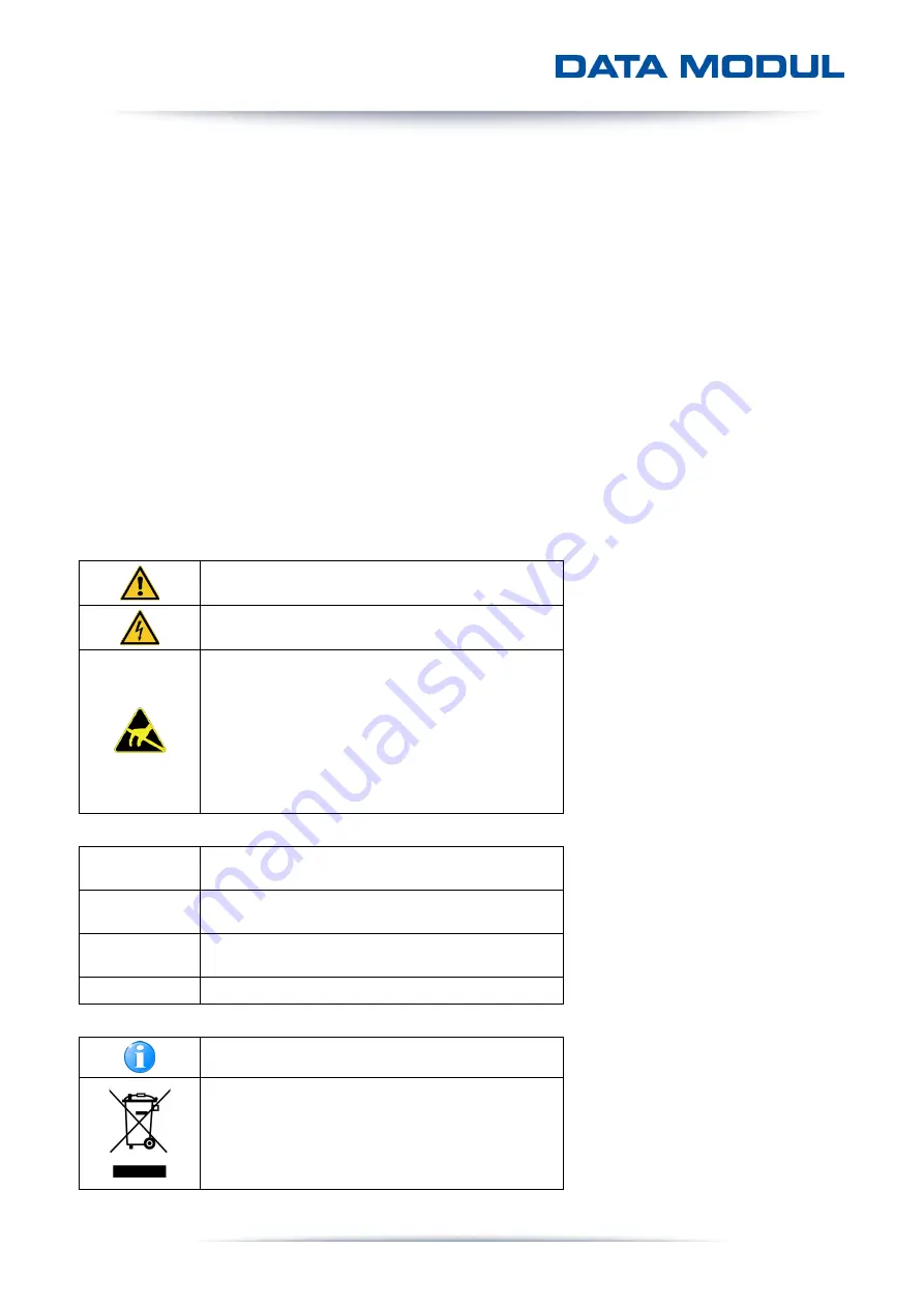
Danger Symbols 


Dangerous Voltage, danger of electric shock 


Hazard point 


All  DATA  MODUL  AG  products  are  electrostatic  sensitive 
devices  and  are  packaged  accordingly.  Do  not  open  or 
handle  a  DATA  MODUL  AG  product  except  at  an 
electrostatic-free workstation. Additionally, do not ship or 
store DATA MODUL AG products near strong electrostatic, 
electromagnetic, magnetic, or radioactive fields unless the 
device  is  contained  within  its  original  manufacturer's 
packaging.  Be  aware  that  failure  to  comply  with  these 
guidelines will void the DATA MODUL AG Limited Warranty. 

Danger Levels 

DANGER 

Indicates a hazardous situation, which will result in death 
or serious injury. 

WARNING 

Indicates  a  hazardous  situation,  which  could  result  in 
death or serious injury. 

CAUTION 

Indicates a hazardous situation, which may result in minor 
or moderate injury. 

NOTICE 

Indicates a property damage. 

General Symbols 


Additional support or useful information. 


The  crossed-out  refuse  bin  indicates  that  the  products 
have to be properly recycled or disposed of in accordance 
with national legislation in the respective EU countries. 
If  you  wish  to  dispose  of  used  electrical  and  electronic 
products outside the European Union, please contact your 
local authority so as to comply with the local regulations. 

Содержание 12040973

Страница 1: ...eDM SBC iMX8Mm SPECIFICATION SAFETY INSTRUCTIONS www data modul com ...

Страница 2: ...is User Manual is merely to provide a better explanation and can differ to the actual appearance of the devices They are to be understood as schematic representations 2020 DATA MODUL AG All rights reserved Trademarks Although all the information contained within this document is carefully checked no guarantee of correctness is implied or expressed All brand or product names are trademarks or regis...

Страница 3: ...s 7 Environmentalism 7 EMC Standards 7 Electrical Safety 7 Shock Vibration 7 Functional Block Diagram 8 Ordering Information 9 Connector Positions 10 Mechanical Design 11 PCB Size 11 Mounting Holes 11 Cooling Solution 12 Platform Features 13 Environmental Conditions 14 Power Supply 14 Input Voltage J5 14 Power over Micro USB 2 0 Type B Connector J16 14 Specifications 14 Power Features 14 Connector...

Страница 4: ...7 22 CPU JTAG Connector J1 optional debug connector 22 External Connectors 23 MicroSD Connector J11 23 Dual USB 2 0 Connector Type A J14 23 Micro USB 2 0 Type B Connector J16 24 Power over Micro USB 2 0 Type B Connector J16 24 Ethernet RJ 45 Connector J18 24 Power Connectors 25 Power In DC Power Jack J5 25 ...

Страница 5: ... Dangerous Voltage danger of electric shock Hazard point All DATA MODUL AG products are electrostatic sensitive devices and are packaged accordingly Do not open or handle a DATA MODUL AG product except at an electrostatic free workstation Additionally do not ship or store DATA MODUL AG products near strong electrostatic electromagnetic magnetic or radioactive fields unless the device is contained ...

Страница 6: ... assist you If you need further assistance after visiting our website please contact our technical support department by email at support data modul com List of Abbreviations Abbreviation Description EMI EN Electro Magnetic Interference European Norm FFC Flat Foil Cable HDMI High Definition Multimedia Interface I2C Inter Integrated Circuit Bus LCD Liquid Crystal Display LVDS NA Low Voltage Differe...

Страница 7: ...ember 2006 of the European parliament and of the council concerning the Registration Evaluation Authorization and Restriction of Chemicals REACH 2012 19 EC of 04 July 2012 directive of the European parliament and of the council on waste electrical and electronic equipment WEEE The board is designed and manufactured to meet ISO 14001 The packing complies with directive 1994 62 EU EMC Standards EMI ...

Страница 8: ...T2 USB2 0 2 RGMII SPI3 I2C4 UART1 or I2S SAI2 USB2 0 1 PCIE color code Standard element connector optional element Block Diagram rev004 LPDDR4 up to 4GB eMMC RTC JTAG Dual USB2 0 Type A x32 x16 LPDDR4 DDR4 DDR3L Up to 3000 MTps Video Processing Unit 2D 3D Vector Graphics 1080p60 Enc Dec 5x I2S SAI 1x PCIe Gen2 1x Gb Ethernet 3x SD eMMC 2x USB2 0 4x UART 1x Quad SPI 3xSPI 4x I2C 4 lane MIPI DSI ARM...

Страница 9: ...porting 5 0 Display Ortustech COM50H5N03ULC eDM SBC iMX8Mm LVDS 12045244 Graphics Module with Dual Channel LVDS USB Touch Backlight eDM SBC iMX8Mm HDMI 12046330 Graphics Module with HDMI 1 2a Type A connector eDM SBC iMX8Mm FIO1 12047960 I O Module with 3 x RS232 1 x RS485 1 x CAN 1 x SPI 1 x I2C 3 x GPIO eDM SBC iMX8Mm SK 12049886 Starterkit with eDM SBC iMX8Mm Q 4G eDM MOD iMX8Mm HDMI Modul eDM ...

Страница 10: ...10 12049720 Rev 01 Draft DATA MODUL AG www data modul com Connector Positions Figure 2 Connector Positions ...

Страница 11: ...0 Rev 01 Draft 11 DATA MODUL AG www data modul com Mechanical Design PCB Size Mechanical dimensions 100mm x 72mm Mounting Holes Figure 3 Mounting Holes Positions Refer to the step file for detailed information ...

Страница 12: ...12 12049720 Rev 01 Draft DATA MODUL AG www data modul com Cooling Solution TBD ...

Страница 13: ...41T62 low power serial real time clock with alarm The battery can be used to provide power backup to the external RTC circuits when external power supply is not available The battery needs to provide a 3V of power and has to be connected to J17 The specified battery type is CR2032 Watchdog Texas Instruments TPS3813 processor supervisory circuit with window watchdog I O Interfaces 2 x USB2 0 Type A...

Страница 14: ... grade Extended temperature ranges on request Temperature storage 40 C 85 C Relative humidity 80 Tolerable air pressure 708 hPa approx altitude 2000m Power Supply Input Voltage J5 VCC 24 0 V 5 or 12 0 V 5 Power over Micro USB 2 0 Type B Connector J16 VCC 5 0 V 10 Specifications Voltage Ripple max 100mV peak to peak 0 20 MHz Rise Time 0 1 20ms from input voltage 10 nominal VCC Max Inrush Current VC...

Страница 15: ...Input I OD 1 8 Bi directional 1 8V Input Output Open Drain I 3 3 3 3V Input I OD 3 3 Bi directional 3 3V Input Output Open Drain I 5 5V Input I OD 5 Bi directional 5V Input Output Open Drain OA Output Analog OD Output Open Drain O 1 8 1 8V Output O 3 3 3 3V Output O 5 5V Output DP I O Differential Pair Input Output DP I Differential Pair Input DP O Differential Pair Output PU Pull Up Resistor PD P...

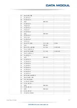
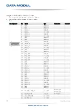
Страница 16: ...V3_M2_S0 3 GND PWR GND 4 V_3V3_M2_S0 5 GND PWR GND 6 M2 B_FULL_CARD_PWROFF_1V8 7 USBHUB_DN3_P 8 M2 B_W_DISABLE1_WWAN_1V8 9 USBHUB_DN3_N 10 M2 B_LED 11 GND PWR GND 12 NC_M2 B_12 13 NC_M2 B_13 14 NC_M2 B_14 15 NC_M2 B_15 16 NC_M2 B_16 17 NC_M2 B_17 18 NC_M2 B_18 19 NC_M2 B_19 20 NC_M2 B_20 21 NC_M2 B_CONFIG0 22 NC_M2 B_22 23 M2 B_WAKE_WWAN_1V8 24 NC_M2 B_24 25 M2 B_DPR_1V8 26 M2 B_W_DISABLE2_GPS_1V8...

Страница 17: ...CIE_RST O 3 3 S0 PD 10K 51 GND PWR GND 52 M2 B_PCIE_CLKREQ I 3 3 S0 PU 10K S0 53 PCIE_CLK_M2_R_N 54 M2 B_PCIE_WAKE I 3 3 S0 PU 10K S0 55 PCIE_CLK_M2_R_P 56 NC_M2 B_56 57 GND PWR GND 58 NC_M2 B_58 59 NC_M2 B_59 60 NC_M2 B_60 61 NC_M2 B_61 62 NC_M2 B_62 63 NC_M2 B_63 64 NC_M2 B_64 65 NC_M2 B_65 66 M2 B_UIM_SIM DETECT 67 M2 B_RESET_1V8 68 CLK_M2_32K768 69 NC_M2 B_CONFIG2 70 V_3V3_M2_S0 71 GND PWR GND...

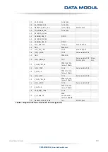
Страница 18: ...ND 9 CSI_D2_P I 1 8 S0 10 DSI_D2_P O 1 8 S0 11 CSI_D2_N I 1 8 S0 12 DSI_D2_N O 1 8 S0 13 GND PWR GND 14 GND PWR GND 15 CSI_CLK_P I 1 8 S0 16 DSI_CLK_P O 1 8 S0 17 CSI_CLK_N I 1 8 S0 18 DSI_CLK_N O 1 8 S0 19 GND PWR GND 20 GND PWR GND 21 CSI_D1_P I 1 8 S0 22 DSI_D1_P O 1 8 S0 23 CSI_D1_N I 1 8 S0 24 DSI_D1_N O 1 8 S0 25 GND PWR GND 26 GND PWR GND 27 CSI_D0_P I 1 8 S0 28 DSI_D0_P O 1 8 S0 29 CSI_D0_...

Страница 19: ...S0 48 I2S_5_MCLK O 1 8 Series resistor 33R 49 GND PWR GND 50 I2S_5_RXD0_R I 1 8 Series resistor 33R PU 10K S0 PU on SOC 51 V_1V8_VDD_S0 PWR 1 8V S0 Imax 100mA 52 I2S_5_TXD0 O 1 8 Series resistor 33R 53 V_3V3_S5 PWR 3 3V S5 Imax 100mA 54 I2S_5_BCLK O 1 8 Series resistor 33R 55 V_3V3_VDD_S0 PWR 3 3V S0 Imax 300mA 56 I2S_5_WCLK O 1 8 Series resistor 33R 57 V_5V0_S0 PWR 5 0V S0 Imax 300mA 58 DSI_RESET...

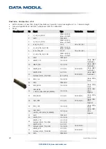
Страница 20: ... Note UART for RS485 10 UART2_TXD O 3 3 S0 Note UART for RS485 11 UART2_RTS I 3 3 S0 PU 10K S0 Note UART for RS485 12 UART2_RXD Optional SAI2_TX_BCLK I 3 3 S0 O 3 3 S0 PU 10K S0 Note UART for RS485 13 SPI2_CLK O 3 3 S0 Note SPI to CAN 14 GND PWR GND 15 SPI2_MOSI O 3 3 S0 Note SPI to CAN 16 CAN_RST GPIO5_IO04 SDIF_RX PWM2 O 3 3 S0 Note CAN CTRL Signals 17 SPI2_MISO I 3 3 S0 PU 10K S0 Note SPI to CA...

Страница 21: ...10K S0 30 SPI3_SCLK O 3 3 S0 31 SPI3_MOSI O 3 3 S0 32 SPI3_CS O 3 3 S0 33 UART3_TXD O 3 3 S0 Note A53 debug console 34 UART4_TXD O 3 3 S0 Note M4 debug console 35 UART3_TXD O 3 3 S0 Note A53 debug console 36 UART4_RXD I 3 3 S0 PU 10K S0 Note M4 debug console 37 GND PWR GND 38 PWRBTN_KEY I 1 8V S0 PU 100K S0 CPU ON OFF Button 39 GND PWR GND 40 RSRBTN_KEY I 5 0V S5 PU 100K S5 System Reset Button Tab...

Страница 22: ...Table 4 RTC Battery Connector Pin Assignment CPU JTAG Connector J1 optional debug connector 1 27mm Pitch Two Rows Pin Header Surface Mount Vertical 10 Circuits Connector type Würth part number 62101021021 Pinout Pin assignment Pin Signal Type Termination Comment 1 JTAG_TMS I 1 8 PU 10k 1 8V S0 2 V_1V8_S0_JTAG PWR 1 8V S0 3 JTAG_TCK I 1 8 PD 10k 4 GND PWR GND 5 JTAG_TDO O 1 8 S0 6 GND PWR GND 7 JTA...

Страница 23: ... 8 6 GND PWR GND 7 SD2_DATA0 I O 3 3 1 8 8 SD2_DATA1 I O 3 3 1 8 9 SD2_CD1_N O 3 3 1 8 0R series resistor and PU 100K 3 3 1 8 PU on SOC 10 SD2_CD2 GND Connected to GND Table 6 MicroSD Connector Pin Assignment Dual USB 2 0 Connector Type A J14 Dual USB 2 0 Conn Type A Connector type Würth 614 008 260 21 or Foxconn UB11121 8FD3 4F Pinout Pin assignment Pin Signal Type Termination Comment 1 V_5V0_USB...

Страница 24: ...or J18 RJ 45 connector with integrated magnetics compliant to Ethernet 1000base Tx and 2 LEDs Connector type TRP Connector 2250015 3 or LINK PP LPJG16414A37NL or W P 655 08 2 60 5 1 8 E Pinout Pin assignment Pin Signal Type Termination Comment 1 GND PWR 1 8V S0 2 ETH_CTREF center tab reference 3 ETH_TRX3_P DP I O 4 ETH_TRX3_N DP I O 5 ETH_TRX2_P DP I O 6 ETH_TRX2_N DP I O 7 ETH_TRX1_P DP I O 8 ETH...

Страница 25: ...C Power Jack J5 DC Power Jack Connector type Kycon KLDHCX 0202 A or Würth 694106301002 or CUI PJ 002AH Pinout Pin assignment Pin Signal Type Termination Comment 1 V_IN_VAR V_in 12V 24V I_max 2 A P_max 24W 12V 12W 24V 2 GND PWR GND 3 GND PWR GND Table 10 Power IN Connector Pin Assignment ...

Страница 26: ...26 12049720 Rev 01 Draft DATA MODUL AG www data modul com ...

Отзывы: