CMOSTEK CMT2300A Скачать руководство пользователя страница 24


CMT2300A 


Rev 1.0 | Page24/46 


www.cmostek.com 

be automatically calibrated during power on and will be periodically calibrated since then. These calibrations will keep the 
frequency tolerance of the oscillator  1%. 
 

4.3.4  Low Battery Detection 

The chip sets up low voltage detection.When the chip is tuned to a certain frequency, the test is performed once.Frequency 
tuning occurs when the chip jumps from the SLEEP/STBY state to the RFS/TFS/TX/RX state. The result can be read by the 
LBD_VALUE register. 
 

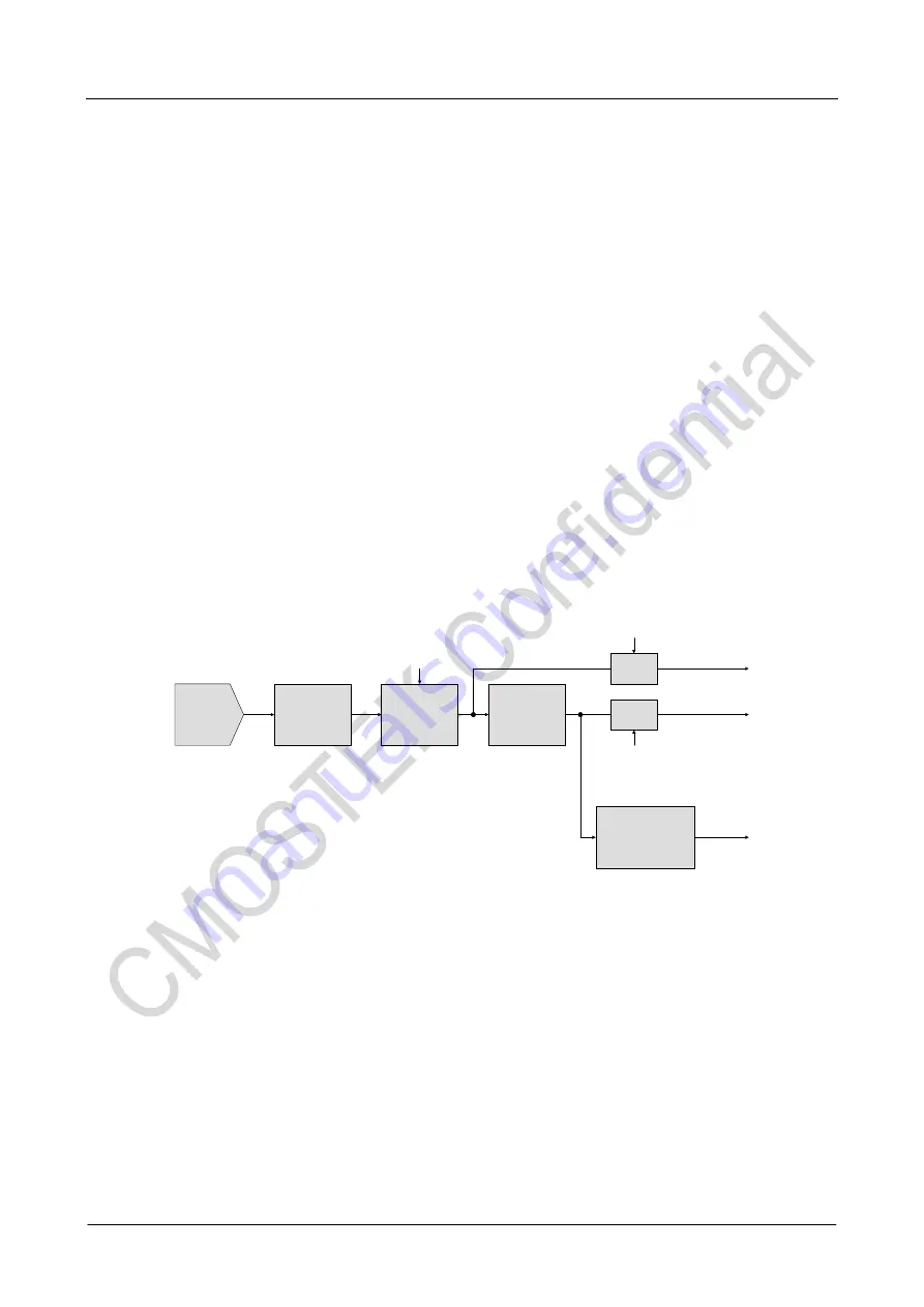
4.3.5  Received Signal Strength Indicator(RSSI) 

RSSI is used to evaluate the signal strengthinside the channel. The cascaded I/Q logarithmic amplifier amplifies the signal before 
it is sent to the demodulator. The logarithmic amplifier of I channels and Q channel contains the received signal indicator, in which 
the DC voltage is generated is proportional to the input signal strength. The output of RSSI is the sum of thevalues of the two 
channels’ signals. The output has 80dB dynamic range above the sensitivity. After the RSSI output is sampled by the ADC and 
filtered by a SAR FILTER and a RSSI AVG FILTER. The order of the average filter can be set by RSSI_AVG_MODE<2:0>. The 
code value is translated into dBm value after filtering. Users can read the registerRSSI_CODE<7:0> to obtain the RSSI code 
value, or RSSI_DBM<7:0> to obtain the dBm value. By setting the register RSSI_DET_SEL<1:0> Users can determine whether 
the RSSI is output to the MCU in real time, or latched at the instance when the preamble, sync, or the whole packet is received.     
 
Also, CMT2300A allows the user to setup a threshold by RSSI_TRIG_TH<7:0> to compare with the real-time RSSI value. If the 
RSSI is larger than the threshold it outputs logic 1, otherwise outputs logic 0. The output can be used as a source of the RSSI 
VLD interrupt, ofthe receive time extending condition in the super low power (SLP) mode. 

SAR 

FILTER

CODE to dBm

CONVERT

SAR 

ADC

RSSI AVG

FILTER

RSSI_CODE<7:0>

RSSI_DBM<7:0>

RSSI_AVG_MODE<2:0>

COMPARE to 

RSSI_TRIG_TH<7:0>

RESULT

LATCH

LATCH

RSSI_DET_SEL<1:0>

RSSI_DET_SEL<1:0>


Figure 7. RSSI detection and comparison circuit


CMT2300A has done a certain degree of calibration before delivery. In order to obtain more accurate RSSI measurement results, 
the user needs to recalibrate the RSSI circuit in their dedicated applications. For further information, please refer to the 
“AN144-CMT2300AW RSSI Usage Guideline”. 
 

4.3.6  Phase Jump Detector

PJD


PJD is Phase Jump Detector. When the chip is in FSK demodulation, itcan automatically observe the phase jump characteristics 
of the received signal to determine whether it is awanted signal or an unwanted noise.   


Содержание CMT2300A

Страница 1: ...16 3 000 pcs For more information see Page 42 Table 23 Descriptions CMT2300A is an ultra low power high performance OOK G FSK RF transceiver suitable for a variety of 140 to 1020 MHz wireless applicat...

Страница 2: ...sitivity VS Temperature 13 1 12 5 Tx Power VS Supply Voltage 13 2 Pin Descriptions 15 3 Typical Application Schematic 17 3 1 Direct tie Schematic Diagram 17 3 2 RF Switch Type Schematic 19 4 Function...

Страница 3: ...35 6 1 Direct Mode 35 6 2 Packet Mode 36 7 Low Power Operation 38 7 1 Duty Cycle Operation Mode 38 7 2 Supper Low Power SLP Receive Mode 38 7 3 Receiver Power VS Performance Configuration 39 8 User Re...

Страница 4: ...2 Absolute Maximum Ratings 1 Parameter Symbol Conditions Min Max Unit Supply Voltage VDD 0 3 3 6 V Interface Voltage VIN 0 3 VDD 0 3 V Junction Temperature TJ 40 125 Storage Temperature TSTG 50 150 So...

Страница 5: ...915 MHz 10 kbps 10 kHz FDEV 8 9 mA RXcurrent low power mode IRx LP FSK 433 MHz 10 kbps 10 kHz FDEV 7 2 mA FSK 868 MHz 10 kbps 10 kHz FDEV 7 3 mA FSK 915 MHz 10 kbps 10 kHz FDEV 7 6 mA TXcurrent ITx FS...

Страница 6: ...Bm DR 20 kbps FDEV 20 kHz Low power setting 109 dBm DR 50 kbps FDEV 25 kHz 108 dBm DR 100 kbps FDEV 50 kHz 105 dBm DR 200 kbps FDEV 100 kHz 102 dBm DR 300 kbps FDEV 100 kHz 99 dBm Sensitivity 915 MHz...

Страница 7: ...2 MHz DR 2 4kbps FDEV 10 kHz 120 3 dBm 433 92 MHz DR 2 4kbps FDEV 20 kHz 119 7 dBm 433 92 MHz DR 9 6 kbps FDEV 9 6 kHz 116 0 dBm 433 92 MHz DR 9 6 kbps FDEV 19 2 kHz 116 1 dBm 433 92 MHz DR 20 kbps FD...

Страница 8: ...t Settle time TSLP RX From Sleep to RX 1000 us TSLP TX From Sleep to TX 1000 us TSTB RX From Standby to RX 350 us TSTB TX From Standby to TX 350 us TRFS RX From RFS to RX 20 us TTFS RX From TFS to TX...

Страница 9: ...rough the coupling capacitor The peak value of the external clock signal is between 0 3V and 0 7V 2 The value includes 1 initial error 2 crystal load 3 aging and 4 change with temperature The acceptab...

Страница 10: ...Digital Interface Table 11 Digital interface specifications Parameter Symbol Condition Min Typ Max Unit Digital input high level VIH 0 8 VDD Digital input low level VIL 0 2 VDD Digital output high le...

Страница 11: ...Voltage Temperature Test Condition Freq 434MHz Fdev 10KHz BR 10Kbps 7 40 7 60 7 80 8 00 8 20 8 40 8 60 8 80 3 6 3 5 3 4 3 3 3 2 3 1 3 0 2 9 2 8 2 7 2 6 2 5 2 4 2 3 2 2 2 1 2 0 1 9 1 8 Current Comsumpt...

Страница 12: ...est Condition FSK DEV 10KHz BR 10Kbps 7 0 7 3 7 5 7 8 8 0 8 3 8 5 8 8 9 0 9 3 9 5 40 25 85 Current Consumption mA Temperature Rx Current vs Volt Temp 3 3V 1 8V 3 6V 117 5 117 0 116 5 116 0 115 5 115 0...

Страница 13: ...Freq 434MHz 20dBm 13dBmmatching network 118 0 117 0 116 0 115 0 114 0 113 0 112 0 40 25 85 Sensitivity dBm Temperature Sensitivity vs Temperature 434MHz 868MHz 10 0 11 0 12 0 13 0 14 0 15 0 16 0 17 0...

Страница 14: ...tion Freq 868MHz 20dBm 13dBmmatching network 9 0 10 0 11 0 12 0 13 0 14 0 15 0 16 0 17 0 18 0 19 0 20 0 3 6 3 5 3 4 3 3 3 2 3 1 3 0 2 9 2 8 2 7 2 6 2 5 2 4 2 3 2 2 2 1 2 1 2 0 1 9 1 8 Tx Power dBm Sup...

Страница 15: ...2300A pin descriptions Pin No Name I O Internal IO Schematic Descriptions 1 RFIP I RF signal input P 2 RFIN I RF signal input N 3 PA O PA output 4 AVDD IO Analog VDD 5 AGND IO Analog GND 6 DGND IO Dig...

Страница 16: ...cuit output 15 1 GPIO2 IO GPIO2 din pd_din dout pd_dout Data tristate pd_din default value is 1 pd_dout default value is 0 VDD Configured as INT1 INT2 DOUT DIN DCLK TX RX and RF_SWT 16 1 GPIO1 IO GPIO...

Страница 17: ...2 2 2 pF C8 5 0603 NP0 50 V 4 7 uF C9 5 0603 NP0 50 V 470 pF C10 5 0603 NP0 50 V 0 1 uF C11 5 0603 NP0 50 V 0 1 uF L1 5 0603 Multilayer chip inductor 180 100 100 nH Sunlord SDCL L2 5 0603 Multilayer...

Страница 18: ...pF C10 5 0603 NP0 50 V 0 1 uF C11 5 0603 NP0 50 V 0 1 uF L1 5 0603 Multilayer chip inductor 180 100 100 nH Sunlord SDCL L2 5 0603 Multilayer chip inductor 22 12 12 nH Sunlord SDCL L3 5 0603 Multilaye...

Страница 19: ...50 V 18nH 220 pF C6 5 0402 NP0 50 V 4 7 2 pF C7 5 0402 NP0 50 V 4 7 2 pF C8 5 0402 NP0 50 V 220 220 uF C9 5 0402 NP0 50 V 220 220 pF C10 5 0402 NP0 50 V 0 1 0 1 uF C11 5 0402 NP0 50 V 0 1 0 1 uF C12 5...

Страница 20: ...tilayer chip inductor 33 22 nH Sunlord SDCL L5 5 0402 Multilayer chip inductor 15 10 nH Sunlord SDCL L6 5 0402 Multilayer chip inductor 27 12 nH Sunlord SDCL L7 5 0402 Multilayer chip inductor 27 12 n...

Страница 21: ...signals to the digital circuit for G FSK demodulation At the same time SARADC will convert the real time RSSI signal to 8 bit digital signal and sent them to the digital part for OOK demodulation and...

Страница 22: ...l is filtered by the image rejection filter and is amplified by the limiting amplifier and then sent to the digital domain for digital demodulation During power on reset POR each analog block is calib...

Страница 23: ...l accurately oscillate at 26 MHz C15 and C16 are the load capacitancesat both ends of the crystal Cpar is the parasitic capacitance on the PCB Each crystal pin has 5pF internal parasitic capacitance t...

Страница 24: ...alue after filtering Users can read the registerRSSI_CODE 7 0 to obtain the RSSI code value or RSSI_DBM 7 0 to obtain the dBm value By setting the register RSSI_DET_SEL 1 0 Users can determine whether...

Страница 25: ...detection and PJD technique they can precisely identify the status of the current channel 4 3 7 Automatic Frequency Control AFC The AFC mechanism allows the receiver to minimize the frequency error be...

Страница 26: ...symbol rate has unexpected changes 4 3 9 Fast Frequency Hopping The mechanism of fast frequency hopping is based on the frequency configured on the RFPDFK for instance 433 92MHz during applications th...

Страница 27: ...sends out the last falling edge of SCLK it must wait for at least half a SCLK cycle and then pull the CSB high To be noticed when reading a register MCU and CMT2300A will have to switch the direction...

Страница 28: ...read write timing diagram Note that there is a slight difference in the control of the FCSB for accessing to the FIFO and the control of the CSB for accessing to the register When the MCU starts to ac...

Страница 29: ...hip usually needs to wait about 1ms then POR will release After the release of the POR the crystal will start the start time is 200 us 1 ms depending on the characteristics of the crystal itself After...

Страница 30: ...ing the register CHIP_MODE_SWT 7 0 5 3 2 OperationState CMT2300A has 7 operationstates IDLE SLEEP STBY RFS RX TFS and TX as shown below Table 16 CMT2300A state and module open table State Binary code...

Страница 31: ...ncreased and the FIFO can be operated The user can choose whether to output CLKO system clock to PIN Because the crystal and LDO is turned on compared to the SLEEP the time switching from the STBY to...

Страница 32: ...to TX requires only 20us Switching from STBY to TX needs to add the PLL calibration and settled time of 350us Switching from SLEEP to TX needs to add the crystal start up and settled time RX can be q...

Страница 33: ...te is written to the RX FIFO Itis a pulse Auto RX_FIFO_OVF 01111 indicates RX FIFO is overflow Auto TX_FIFO_NMTY 10000 Indicates that TX FIFO is not empty Auto TX_FIFO_TH 10001 Indicates the number of...

Страница 34: ...2 GPO1_SEL 1 0 GPIO1 0 Preamble OK Interrupt Source 0 Sycn Word OK Interrupt Source 0 Node ID OK Interrupt Source 0 CRC OK Interrupt Source 0 Packet OK Interrupt Source 0 Sleep Timeout Interrupt Sourc...

Страница 35: ...1 2 or 3 The typicalRX direct mode controlsequencefor the MCU is 1 Configures GPIOsusing theCUS_IO_SEL register 2 Configures DATA_MODE 0 3 Send thego_rx command 4 Capture the data from DOUT continuous...

Страница 36: ...t format Length in front of the Node ID variable packet format Length in the back of the Node ID and fixed packet format Each element in the packet supports flexible configurations as shown below Prea...

Страница 37: ...go_sleep go_stby go_rfs command to stop the receiving and save the power 6 Clears the packet interruptsusingCUS_ INT_CLR1 and CUS_INT_CLR2 registers Tx processing In the packet mode MCU can fill the d...

Страница 38: ...ption under different application requirements These options can be used whensetting RX_TIMER_EN to 1 e g when the Rx timer is enabled The principle of the SLP mechanism is to shorten the Rx time when...

Страница 39: ...one of PREAM_OK or NODE_OK is valid 10 Any one of PREAM_OK or SYNC_OK or NODE_OK is valid 11 Once meet the Rx extended condition during T1 switch to T2 Leave T2 and pass the control authority to MCU a...

Страница 40: ...X8 0x5D RW CUS_TX9 0x5E RW CUS_TX10 0x5F RW CUS_LBD Addr R W Name Bit 7 Bit 6 Bit 5 Bit 4 Bit 3 Bit 2 Bit 1 Bit 0 Function 0x60 RW CUS_MODE_CTL 0x61 RW CUS_MODE_STA RESV RESV RSTN_IN_EN CFG_RETAIN 0x6...

Страница 41: ...deviation and power 0x60 0x6A Control Bank 1 Set by MCU in application not generated by RFPDK To setup chip working state frequency hopping GPIOs and interrupts control 0x6B 0x71 Control Bank 1 Set by...

Страница 42: ...ower Sub 1GHz RF Transceiver QFN16 3x3 Tape Reel 1 8 to 3 6V 40 to 85 3 000 Note 1 E represents extended industrial grade The temperature range is from 40 to 85 Q represents QFN16 packaging R represen...

Страница 43: ...kaging information is as below D2 E2 b e L D E A A1 c Top View Bottom View Side View 1 1 16 16 Figure 24 16 Pin QFN 3x3 packaging Table 24 16 Pin QFN 3x3 Packaging Size Symbol Size mm Min Max A 0 7 0...

Страница 44: ...king description Marking method Laser Pin 1 mark Circle diameter 0 3 mm Font size 0 5 mm right aligned Line 1 marking 300A represents model CMT2300A Line 2 marking represents the internal tracking cod...

Страница 45: ...pter 5 and 6 from Chapter 4 2015 08 06 0 7 All Initial release for production version 2017 03 22 0 8 All Changed T R to 3 000 pcs Added AN document list Added new RF parameters and curves 2017 08 10 0...

Страница 46: ...ty is assumed for inaccuracies and specifications within this document are subject to change without notice The material contained herein is the exclusive property of CMOSTEK and shall not be distribu...

Отзывы: