


CR10X User Guide
6-6
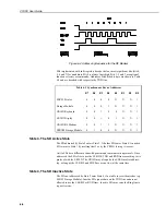
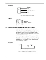
Figure 6-4 Addressing Sequence for the RF Modem
SDs implemented with shift registers decode the four most significant bits (bits 4,
5, 6 and 7) for an address. Bit 0 is always logic high. Bits 1, 2 and 3 are optional
function selectors or commands. Addresses established to date are shown in Table
6-2 and are decoded with respect to the TXD line.
Table 6-2 Synchronous Device Addresses
B7
B6
B5
B4
B3
B2
B1
B0
SDC99 Printer
0
0
0
0
X
X
X
1
Storage Module
0
0
0
1
X
X
X
1
CR10X Keyboard
0
0
1
0
0
X
X
1
CR10X Display
0
0
1
0
1
X
X
1
CR10X RF Modem
0
0
1
1
X
X
X
1
EPROM Storage Module
0
1
0
0
X
X
X
1
State 3, The SD Active State
The SD addressed by State 2 enters State 3. All other SDs enter State 4. An active
SD returns to State 1 by resetting itself, or by the CR10X forcing it to reset.
Active SDs have different acknowledgement and communication protocols. Once
addressed, the SD is free to use the CLK/HS, TXD and RXD lines according to its
protocol with the CR10X. The CR10X may also pulse the SDE line after address-
ing, as long as the CLK/HS and SDE lines are not low at the same time.
State 4, The SD Inactive State
The SDs not addressed by State 2 enter State 4, if not able to reset themselves (e.g.
SM192 Storage Module). Inactive SDs ignore data on the TXD line and are not
allowed to use the CLK/HS or RXD lines. Inactive SDs may raise the Ring line to
request service.