


www.austriamicrosystems.com
Revision 1.10
48 - 86
AS3542 3v2
Data Sheet, Strictly Confidential - D e ta i l e d D e s c r i p t i o n - S Y S T E M F u n c t i o n s
10.6.3 Parameter
AVDD27=2.7, T
A
= 25
o
C, unless otherwise mentioned
10.6.4 Register Description
10.7 GPIO Pins
10.7.1 General
PWGD, XRES, SDO, XIRQ are so called GPIO (general purpose inputs/outputs) as they can feature auxiliary function-
ality.
If the main pin function is not needed all pins can provide internal clocks or can drive a static HIGH or LOW. Four differ-
ent clock lines (CLKINT1, CLKINT2, CLK24M, CLK32K) can be selected. Each of these clock lines can drive different
frequencies which can be set by register options. In addition some pins can provide a PWM signal. The duty cycle of
the PWM output can also be set in the registers.
PWGD, XRES and XIRQ can be configured also as open drain outputs. For all pins the driver strength of the push/pull
output mode can be selected.
PWGD, Q24M, Q32K can also be used as inputs for a heartbeat signal or an external dimming signal for the DCDC15
booster.
10.7.2 Internal Source Signals
CLKINT1 Signal
This is an internal signal line which can drive pre defined frequencies of 125Hz, 1kHz, 667kHz or 2MHz. This signal
line can be selected as source for the XRES, XIRQ and SDO GPIO output pins.
CLKINT2 Signal
This is an internal signal line which can drive the PLL clock, the clock for the logarithmic dimming of DCDC15 or can
be set to static HIGH/LOW. This signal line can be selected as source for the PWGD and XIRQ output pins.
PWM Signal
The duty cycle of the PWM signal can be set in 128 steps plus an option to invert the signal. It ca be used as source for
all GPIO outputs other than XIRQ.
10.7.3 Pin Functions
PWGD Pin
Can drive CLKINT2 or the PWM signal as auxiliary function. The output can be configured to operate in push/pull (2
different driver strength) open-drain mode or to be trie-state. It can be used as an input for a heartbeat, external dim-
ming signal or as additional source for the 10-bit general purpose ADC.
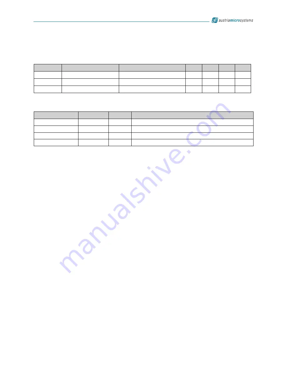
Table 37. ADC10 Parameter
Symbol
Parameter
Condition
Min
Typ
Max
Unit
ADC
FS
ADC Full Scale Range
-
2.16
-
V
T
CON
Conversion Time
-
34
50
µs
I_MIC
FS
I_MICS Full Scale Range
0.7
1.0
1.4
mA
Table 38. ADC10 Related Register
Name
Base
Offset
Description
2-wire serial
1Ch
Extended ADC source selection
2-wire serial
27h
Interrupt settings for end of conversion interrupt
2-wire serial
2Eh
ADC source selection, ADC result<9:8>
2 wire serial
2Fh
ADC result <7:0>