background image

4-10

SAM9N12/CN11-EK User Guide

11186A–ATARM–29-Nov-12

A 3-state buffer is in serial with NAND flash’s CE signal, with PB1 to give a manually disable manner for 
NAND boot.

4.3.8

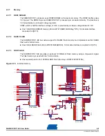
UART DBGU

The Universal Asynchronous Receiver Transmitter features a two-pin UART that can be used for com-
munication and trace purposes and offers an ideal medium for in-situ programming solutions.

This two-pin UART (TXD and RXD only) is buffered through an RS232 transceiver MN16 and brought to 
the DB9 male connector J11.

Figure 4-11.  UART

4.3.9

JTAG Interface

The SAM9N12/CN11-EK board includes a JTAG interface port (J4), to provide debug level access to the 
processor. The JTAG port is a 20-pin male connector. This port provides the required interface for in-cir-
cuit emulators such as ARM’s Multi-ICE.

Figure 4-12.  JTAG


VD DI OP0

R136
100K

R 135
100K

C 91
100nF

C 94
100nF

MN 16
MAX3232CSE

T1IN

11

T2IN

10

R1O UT

12

R2O UT

9

T1OU T

14

T2OU T

7

R 1I N

13

R 2I N

8

V+

2

C1+

1

C1-

3

C2+

4

C2-

5

V-

6

VCC

16

GND

15

C92
100nF

C 93
100nF

C90

100nF

J 11

5

4

3

2

1

9

8

7

6

10

11

PA10

(D TXD)

UART

PA9

(D RXD)

VDD I OP0

Содержание SAM9N12/CN11-EK

Страница 1: ...11186A ATARM 29 Nov 12 SAM9N12 CN11 EK User Guide ...

Страница 2: ...t 3 1 3 4 Recovery Procedure 3 1 Section 4 Evaluation Kit Hardware 4 1 4 1 Board Overview 4 1 4 2 Equipment List 4 2 4 2 1 Features List 4 2 4 2 2 Interface Connection 4 3 4 2 3 Configuration Items 4 3 4 3 Function Blocks 4 5 4 3 1 Processor 4 5 4 3 2 Clock Distribution 4 5 4 3 3 Reset and Wake up Circuitry 4 6 4 3 4 Power Supplies 4 6 4 3 5 Power Rails 4 7 4 3 6 Battery Backup 4 8 4 3 7 Memory 4 ...

Страница 3: ...5 4 4 5 USB Type A port 4 25 4 4 6 SD Card MCI 4 26 4 4 7 Ethernet RJ45 Socket 4 27 4 4 8 Zigbee Socket J12 4 27 4 4 9 LCD Socket 4 28 4 4 10 IO Expansion Port 4 30 Section 5 EK Schematics 5 1 5 1 SAM9N12 EK Schematics 5 1 5 2 SAM9CN11 EK Schematics 5 2 Section 6 Display Module Hardware 6 1 6 1 Board Overview 6 1 6 2 Equipment List 6 1 6 3 Function Blocks 6 2 6 3 1 3 3V Regulator 6 2 6 3 2 TFT LCD...

Страница 4: ...SAM9N12 CN11 EK User Guide 1 3 11186A ATARM 29 Nov 12 8 1 Revision History 8 1 ...

Страница 5: ...esigns SAM9N12 CN11 Evaluation Kit consists of two boards The Evaluation Kit EK board The Display Module DM board 1 2 User Guide Content This guide gives details on how the SAM9N12 CN11 EK has been designed It is made up of 8 sections Section 1 Introduction including references applicable documents Section 2 Kit Contents Section 3 Power Up Section 4 Evaluation Kit Hardware Section 5 EK Schematics ...

Страница 6: ...tains the following items Board One SAM9N12 CN11 EK board One SAM9N12 CN11 DM board Power supply Universal input AC DC power supply with US Europe and UK plug adapters One 3V lithium battery type CR1225 Cables One serial RS232 cable One micro A B type USB cable One RJ45 crossed cable A Welcome letter Figure 2 1 Unpacked SAM9N12 CN11 EK ...

Страница 7: ...trap or similar ESD protective device when handling the board in hostile ESD environments offices with syn thetic carpet for example Avoid touching the component pins or any other metallic element on the board Table 2 1 SAM9N12 CN11 Evaluation Kit Specifications Characteristics Specifications Clock speed 400 MHz PCK 133 MHz MCK Ports Ethernet USB RS232 JTAG Audio SD card Board supply voltage 5V DC...

Страница 8: ... of the SAM9N12 CN11 devices when the board is switched off 3 3 Sample Code and Technical Support After boot up designers can run sample code or their own application on the development kit Users can download sample code and get technical support from the Atmel web site http www atmel com 3 4 Recovery Procedure All boards of Evaluation Kit have passed strict test procedures before shipment The dem...

Страница 9: ...epts such as power distribution memory and interface assignments The SAM9N12 CN11 EK board is built around on the integration of an ARM 926 based microcontroller BGA 217 package with on board SDRAM NAND Flash and a set of popular peripherals It is designed to provide a high performance processor evaluation solution with high flexibility for various kinds of applications Figure 4 1 SAM9N12 Board Ar...

Страница 10: ...ist Here is the list of the EK board components SAM9N12 CN11 microcontroller BGA 16 MHz crystal 32 768 kHz crystal Memory 1 Gbit DDR2 memory 2 Gbits NAND Flash memory with chip selection control switch Optional NOR Flash 32 Mbits SPI serial DataFlash with chip selection control switch 512 Kbits serial EEPROM 1 Kbit 1 Wire EEPROM ...

Страница 11: ...K board includes hardware interfaces such as DC power supply J1 Backup battery Bt1 USB host type A connector J2 USB device micro B connector J3 One Ethernet 10 100 interface through an ETH controller J16 DBGU RX and TX only connected to a 9 way male RS232 connector J11 JTAG 20 pin IDC connector J4 SD connector J8 Headphone J13 line in J15 on board mic phone mic1 DM board connection for QTouch and ...

Страница 12: ...4 4 SAM9N12 CN11 EK User Guide 11186A ATARM 29 Nov 12 Figure 4 3 SAM9N12 EK Board Layout ...

Страница 13: ...M9N12 CN11 device in BGA217 package The processor runs at a nominal frequency of 400 MHz for the core and 133 MHz for the system bus 4 3 2 Clock Distribution The SAM9N12 CN11 EK board includes three clock systems Two of the clock systems are alternatives for the SAM9N12 CN11 main clock and one clock system is an oscillator used for the Ethernet controller chip ...

Страница 14: ...CN11 EK board evaluation and development platform embeds all the necessary power rails required for the SAM9N12 CN11 processor and peripherals The SAM9N12 CN11 EK board can be supplied by either a USB connection via J3 or a 5V DC block through input J1 refer to usb schematic A manual power supply selection SW1 between the USB supply and the 5V power supply is provided to select the main power line...

Страница 15: ...er regulated to 3 3V The main 3 3V regulator is based on a RICHTEK RT9018A low dropout regulator providing a fixed output of 3 3V Its output is used for VDDIOP0 VDDIOP1 VDDANA VDDOSC VDDUSB VDDFUSE When the 3 3V supply is present power LED D10 is lit Test points TP2 to TP5 are used to perform testing Figure 4 6 3 3V Supply Table 4 2 Power Input Configuration PIN INPUT 1 Center Positive 2 No connec...

Страница 16: ...upply 4 3 6 Battery Backup VDDBU pin is powered from the 3 3V rail and a backup battery BT1 via a dual Schottky diode D1 Test point TP13 and jumper JP2 are used to perform testing Figure 4 9 Backup Battery Note Test points TPn are provided for easy access to each of the regulated power lines PWR_EN TP7 VDDNF L5 220ohm at 100MHz 1 2 C9 10uF C8 4 7uF 5V 1V8 MN2 LP38692MP 1 8 VIN 4 VOUT 3 VEN 1 NC 2 ...

Страница 17: ...0 DQ14 52 DQ15 54 VCC 33 VCCQ 38 VPP 43 VSS 28 VSS 31 VSS 12 A21 11 NC 13 CE 30 OE 32 WE 14 RST 44 WP 15 CLK 45 WAIT 56 A22 10 A23 9 RFU2 27 RFU1 26 ADV 46 DDR2_NCS1 DDR2_CAS R72 100K R71 100K DDR2_RAS DDR2_DQS1 DDR2_SDWE DDR2_DQS0 F LASH_A22 DDR2_DQM 1 DDR2_DQM 0 NANDCS FLASH_D 0 15 1V8 MN15 NL17SZ126 OE 1 VCC 5 GND 3 OUT 4 IN 2 C82 100nF OE_Nandflash NRD NWRE NCS0 JP9 R73 470K F LASH_A23 C83 100...

Страница 18: ...RS232 transceiver MN16 and brought to the DB9 male connector J11 Figure 4 11 UART 4 3 9 JTAG Interface The SAM9N12 CN11 EK board includes a JTAG interface port J4 to provide debug level access to the processor The JTAG port is a 20 pin male connector This port provides the required interface for in cir cuit emulators such as ARM s Multi ICE Figure 4 12 JTAG VD DIOP0 R136 100K R 135 100K C 91 100nF...

Страница 19: ... the industry standard I2C interfaces On the EK board TWI0 port is used to interface with serial EEPROM QTouch device and audio CODEC interface SAM9N12 CN11 processor supports TWI EEPROM boot at the device address of 0x50 On board the EEPROM device address is 0x51 Customer needs to dismount R61 and mount R62 as 10 kohms if EEPROM boot is needed Figure 4 14 EEPROM R56 0R R57 0R R58 0R VDDIOP0 VDDIO...

Страница 20: ...equipped with 500 mA power switch for bus powered applications Figure 4 15 USB Port TP12 5V C37 10uF C32 10pF D6 TVS 1 2 D5 TVS 1 2 R16 0R R17 0R R18 0R R19 0R D4 TVS 1 2 USB_A J2 USB AF 4 1 4 5 2 3 6 USB_ 5V PC31 RV1 V5 5MLA0603 PB8 VBUS SHD DM DP ID GND J3 USB Micro B 1 2 3 4 5 7 6 8 9 C31 100nF R21 27R R20 27R R24 27R R25 27R R26 47K MN6 SP2526A 2 ENA 1 FLGA 2 ENB 4 OUTA 8 GNG 6 FLGB 3 IN 7 OUT...

Страница 21: ...2 220 ohm at 100 MHz 1 2 ETH_ D3 ETH_ D2 3V3 R1 84 470 R C12 7 100 nF C 128 1 00n F C1 29 10 0nF R1 86 470 R ETH_ D7 ETH_ D6 ETH_ D5 ETH_ D4 C 131 1 00n F Y3 25M Hz 1 2 3 4 R18 5 3 01 K 1 GND_ ETH G ND_ ETH 1V8 M N20 SN 74LVC 1G07 N C 1 A 2 GND 3 Y 4 VCC 5 ETH_ D11 ETH_ D10 ETH_ D9 ETH_ D8 ETH_ D15 ETH_ D14 ETH_ D13 ETH_ D12 C1 26 10 uF C13 2 4 7 uF R 177 4 9 9 R 1 R 176 49 9R 1 1V8 C13 6 100 nF G...

Страница 22: ...WD0 PA31 PA30 TWCK0 L19 220ohm at 100MHz 1 2 3V3 AVDD1V8 C100 10uF AGND_AUDIO AVDD1V8 MN17 WM8904 SCLK 2 SDA 3 MCLK 28 BCLK GPIO4 29 IN1L DMICDAT1 27 IN1R DMICDAT2 25 I N2L 26 IN2R 24 DGND 5 LRCLK 30 DACDAT 32 ADCDAT 31 GPIO1 IRQ 1 HPOUTL 13 HPOUT R 15 HPOUTFB 14 LINEOUTL 16 LINEOUT R 18 LINEOUTFB 17 CPVDD 7 CPCA 8 CPCB 10 CPVOUTP 11 CPVOUTN 12 M ICB I AS 20 MICVDD 19 CPGND 9 VM I DC 21 AVDD 23 DC...

Страница 23: ... application Figure 4 20 ZigBee MCI_CDA PA19 UP TOUCH SD CARD J8 SD P09KC M1 Up Touch Connector DAT1 RSV 8 DAT0 DO 7 VSS2 6 CLK SCLK 5 VDD 4 VSS1 3 CMD DI 2 CD DAT3 CS 1 DAT2 RSV 9 nCD 10 WP 11 Shell1 12 Shell2 13 SD CARD PA7 R84 68K R106 27R R110 27R C89 100nF R83 10K R85 68K PA16 PA17 R86 68K R87 68K R88 68K MCI_DA3 VDDIOP0 MCI_DA2 RR26A 1 8 RR26B 2 7 RR26C 3 6 MCI card detect RR26D 4 5 MCI_DA1 ...

Страница 24: ... debugging or to implement an analog user control such as display brightness vol ume etc Figure 4 22 Potentiometer 4 3 19 LED Indicators There are three LEDs for general purpose on the SAM9N12 CN11 EK board D8 blue and D9 green LEDs are user defined and controlled by the GPIO D10 red LED is a power LED indicating that the 3 3V rail is enabled It can also be controlled by the GPIO by default the GP...

Страница 25: ... ROM code whatever the contents of the NAND Flash or serial DataFlash Please refer to SAM9N12 CN11 datasheet boot strategy for details Figure 4 24 PB1 4 3 20 2 PB2 NRST The NRST pin is bidirectional It is handled by the on chip reset controller and can be driven low to pro vide a reset signal to the external components or be asserted low externally to reset the microcontroller It will reset the co...

Страница 26: ...PD10 PD8 PD7 PD9 PD 10 PD 8 PD 7 PD 9 PD6 PD 6 PD 11 3V3 PD12 PD13 PD 13 PD 12 JP8 1 2 3 3V3 5V LCDDAT4 PB11 PB15 PB13 PC19 LCDDAT21 3V3 PC1 5V_LCD LCD_DETECT LCD_DET LCDDAT9 PA30 PC21 TWCK0 SPI1_MISO LCDDAT6 PB0 PB9 PA23 PA21 PC3 AD1_XM LCDDAT23 LCDDAT11 LCDHSY NC PC14 LCDDAT0 TWD0 VDDANA SPI1_MOSI LCDDAT10 PC23 R111 22R R114 22R PC28 PC26 R113 22R R112 22R PC30 AD2_YP LCDDAT16 PC13 R115 22R R117...

Страница 27: ...S0 ZigBee PA9 DRXD DBGU PA10 DTXD DBGU PA11 SPI0_MISO MCI_DA4 Serial DataFlash PA12 SPI0_MOSI MCI_DA5 Serial DataFlash PA13 SPI0_SPCK MCI_DA6 Serial DataFlash PA14 SPI0_NPCS0 MCI_DA7 Serial DataFlash PA15 MCI_DA0 MCI PA16 MCI_CDA MCI PA17 MCI_CK MCI PA18 MCI_DA1 MCI PA19 MCI_DA2 MCI PA20 MCI_DA3 MCI PA21 TIOA0 SPI1_MISO ZigBee PA22 TIOA1 SPI1_MOSI ZigBee PA23 TIOA2 SPI1_SPCK ZigBee PA24 TCLK0 TK A...

Страница 28: ... PB0 RTS2 LCD connector PB1 CTS2 LCD connector PB2 SCK2 JUMPER to GND PB3 SPI0_NPCS3 PB_USER1 PB4 USER_LED1 PB5 USER_LED2 PB6 AD7 PWR_LED PB7 AD8 EN5V_HOST PB8 AD9 OVCUR_USB PB9 AD10 PCK1 LCD connector PB10 AD11 PCK0 Audio PB11 AD0 PWM0 TSC PB12 AD1 PWM1 TSC PB13 AD2 PWM2 TSC PB14 AD3 PWM3 TSC PB15 AD4 TSC PB16 AD5 VBUS_SENSE PB17 AD6 Analog input PB18 IRQ ADTRG LCDHSYNC 0R ...

Страница 29: ...4 LCD PC8 LCDDAT8 UTXD0 LCD PC9 LCDDAT9 URXD0 LCD PC10 LCDDAT10 PWM0 LCD PC11 LCDDAT11 PWM1 LCD PC12 LCDDAT12 TIOA5 LCD PC13 LCDDAT13 TIOB5 LCD PC14 LCDDAT14 TCLK5 LCD PC15 LCDDAT15 PCK0 LCD PC16 LCDDAT16 UTXD1 LCD PC17 LCDDAT17 URXD1 LCD PC18 LCDDAT18 PWM0 LCD PC19 LCDDAT19 PWM1 LCD PC20 LCDDAT20 PWM2 LCD PC21 LCDDAT21 PWM3 LCD PC22 LCDDAT22 TXD3 LCD PC23 LCDDAT23 RXD3 LCD PC24 LCDDISP RTS3 LCD P...

Страница 30: ...E NAND Flash PD1 NANDWE NAND Flash PD2 A21 NANDALE NAND Flash PD3 A22 NANDCLE NAND Flash PD4 NCS3 NAND Flash PD5 NWAIT PD6 D16 NAND Flash PD7 D17 NAND Flash PD8 D18 NAND Flash PD9 D19 NAND Flash PD10 D20 NAND Flash PD11 D21 NAND Flash PD12 D22 NAND Flash PD13 D23 NAND Flash PD14 D24 PD15 D25 A20 PD16 D26 A23 PD17 D27 A24 PD18 D28 A25 PD19 D29 NCS2 PD20 D30 NCS4 PD21 D31 NCS5 ETH INT ...

Страница 31: ... to create the logic level reference for the input comparators and to control the output logic levels to the target It is normally fed from VDD on the target board and must not have a series resistor 2 Vsupply 3 3V power This pin is not connected in SAM ICE It is reserved for compatibility with other equipment Connect to VDD or leave open in target system 3 nTRST TARGET RESET Active low output sig...

Страница 32: ...nded that this pin is pulled to a defined state on the target board Typically connected to TCK on target CPU 10 GND Common ground 11 RTCK Input return test clock signal from the target Some targets must synchronize the JTAG inputs to internal clocks To assist in meeting this requirement a returned and retimed TCK can be used to dynamically control the TCK rate SAM ICE supports adaptive clocking wh...

Страница 33: ... 32 USB Type A Port J2 Pin Mnemonic PIO Via translator Description 1 4 6 9 No connection 2 RXD Received Data PA9 RS232 serial data output signal 3 TXD Transmitted Data PA10 RS232 serial data input signal 5 GND Common ground 7 RTS Request To Send Not used 8 CTS Clear To Send Not used Mechanical pins Shield Pin Mnemonic Description 1 Vbus 5V power 2 DM Data minus 3 DP Data plus 4 ID On the go identi...

Страница 34: ...MMC Socket J8 Table 4 12 SD Socket J8 Signal Descriptions Pin Mnemonic Description 1 Vbus 5V power 2 DM Data minus 3 DP Data plus 4 GND Common ground 5 6 Shield Mechanical pins Pin Function PIO 1 MCI_DA3 PA20 2 MCI_CMD PA16 3 GND 4 VDDIOP0 5 MCI_CLK PA17 6 GND 7 MCI_DA0 PA15 8 MCI_DA1 PA18 9 MCI_DA2 PA19 10 MCI_CD PA7 11 WP 12 GND 13 GND ...

Страница 35: ...ignal Descriptions Pin Mnemonic Description 1 TX Differential output plus 2 TX Differential output minus 3 RX Differential input plus 4 Reserved 5 Reserved 6 RX Differential input minus 7 Reserved 8 Reserved Function Signal Name Port Pin Pin Port Signal Name Function Reset RST 1 2 IRQ0 Interrupt Request Interrupt Request IRQ1 3 4 SLP_TR SLP_TR SPI chip select CS 5 6 MOSI SPI MOSI SPI MISO MISO 7 8...

Страница 36: ...ND ZB_IRQ0 ZB_IRQ0 5 6 ZB_IRQ1 TWCK0 TWCK0 7 8 TWD0 GND GND 9 10 ISI_MCK LCDDAT15 GND GND 11 12 ISI_VSYNC LCDDAT13 GND GND 13 14 ISI_HSYNC LCDDAT14 GND GND 15 16 ISI_PCK LCDDAT12 GND GND 17 18 ISI_D0 LCDDAT0 LCDDAT1 ISI_D1 19 20 ISI_D2 LCDDAT2 LCDDAT3 ISI_D3 21 22 ISI_D4 LCDDAT4 LCDDAT5 ISI_D5 23 24 ISI_D6 LCDDAT6 LCDDAT7 ISI_D7 25 26 ISI_D8 LCDDAT8 LCDDAT9 ISI_D9 27 28 ISI_D10 LCDDAT10 LCDDAT11 I...

Страница 37: ... LCDDAT18 7 8 LCDDAT19 LCDDAT20 9 10 LCDDAT21 LCDDAT22 11 12 LCDDAT23 GND GND 13 14 GND GND LCDDISP 15 16 LCDPWM LCDCSYNC 17 18 LCDHSYNC LCDDEN 19 20 LCDPCK GND GND 21 22 GND GND AD0_XP TSC 23 24 TSC AD1_XM AD2_YP TSC 25 26 TSC AD3_YM AD4_LR TSC 27 28 ONE_WIRE GND GND 29 30 GND GND SPI1_MISO 31 32 SPI1_MOSI SPI1_SPCK 33 34 SPI1_NPCS1 EN_PWRLCD SELCONFIG 35 36 LCD_DETEC T LCD_DETECT PD16 37 38 PD17...

Страница 38: ...l Descriptions PIO Power Pin Num Pin Num Power PIO 3V3 or 5V 1 2 3V3 or 5V GND 3 4 GND PA0 5 6 PA16 PA1 7 8 PA17 PA2 9 10 PA18 PA3 11 12 PA19 PA4 13 14 PA20 PA5 15 16 PA21 PA6 17 18 PA22 PA7 19 20 PA23 PA8 21 22 PA24 PA9 23 24 PA25 PA10 25 26 PA26 PA11 27 28 PA27 PA12 29 30 PA28 PA13 31 32 PA29 PA14 33 34 PA30 PA15 35 36 PA31 GND 37 38 GND 3V3 39 40 3V3 ...

Страница 39: ...ons PIO Power Pin Num Pin Num Power PIO 3V3 or 5V 1 2 3V3 or 5V GND 3 4 GND PB0 5 6 PB16 PB1 7 8 PB17 PB2 9 10 PB18 PB3 11 12 PD6 PB4 13 14 PD7 PB5 15 16 PD8 PB6 17 18 PD9 PB7 19 20 PD10 PB8 21 22 PD11 PB9 23 24 PD12 PB10 25 26 PD13 PB11 27 28 PD14 PB12 29 30 PD17 PB13 31 32 PD18 PB14 33 34 PD19 PB15 35 36 PD20 GND 37 38 PD21 3V3 39 40 3V3 ...

Страница 40: ...ns PIO Power Pin Num Pin Num Power PIO 3V3 or 5V 1 2 3V3 or 5V GND 3 4 GND PC0 5 6 PC16 PC1 7 8 PC17 PC2 9 10 PC18 PC3 11 12 PC19 PC4 13 14 PC20 PC5 15 16 PC21 PC6 17 18 PC22 PC7 19 20 PC23 PC8 21 22 PC24 PC9 23 24 PC25 PC10 25 26 PC26 PC11 27 28 PC27 PC12 29 30 PC28 PC13 31 32 PC29 PC14 33 34 PC30 PC15 35 36 PC31 GND 37 38 GND 3V3 39 40 3V3 ...

Страница 41: ... 1 11186A ATARM 29 Nov 12 Section 5 EK Schematics 5 1 SAM9N12 EK Schematics This section contains the following schematics Top Level Power Supply AT91SAM9N12 EBI Interface PIO Interfaces DDR2 NAND Flash Serial Interfaces Audio ETH ...

Страница 42: ...tect SPI0_MISO SPI1_NPCS0 SPI0_MOSI DRXD SPI0_SPCK SPI0_NPCS0 MCI_DA0 MCI_DA3 TWCKO SPI1_MISO SPI1_MOSI SPI1_SPCK TK TF TD MCI_CDA RD MCI_CK RK MCI_DA1 RF MCI_DA2 TWD0 PWR_LE EN5V_HOST OVCUR_USB PCK0 AD0 AD1 AD2 AD3 AD4 VBUS_SENSE AD6 ADTRG ROM CODE PB_USER1 USER_LED1 USER_LED2 LCDDAT7 LCDDAT8 LCDPCK LCDDAT9 LCDDAT20 OVCUR_LCD LCDDAT10 LCDDAT21 LCDDAT11 LCDDAT22 LCDDAT12 LCDDAT23 LCDDAT13 LCDDISP ...

Страница 43: ...ose offender to legal proceedings INIT EDIT A B C EBI NOR NRST 2 9 C XX XXX XX PP XXX POWER SUPPLY 20 AUG 11 SAM9N12 EK_RevC BGA217 25 NOV 11 25 SEPT 11 XXX XXX XX XXX XX XX XXX XX PP PP R4 100K R4 100K MN1 RT9018A MN1 RT9018A PGOOD 1 EN 2 VIN 3 VDD 4 NC 5 VOUT 6 ADJ 7 GND 8 GND 9 R10 12K 1 R10 12K 1 TP3 TP3 C4 10uF C4 10uF R2 47K R2 47K SW1 SW SLIDE 3 SW1 SW SLIDE 3 3 1 2 R1 100K R1 100K MN2 LP38...

Страница 44: ... B2 GNDPLL P14 VDDNF J14 VDDNF K14 VDDIOM H10 VDDIOM H9 VDDIOM H8 GNDBU B3 VDDANA C4 ADVREF A2 VDDPLL T16 GNDCORE D8 VDDBU D6 VDDUSB R15 VDDCORE J4 VDDCORE G15 VDDCORE C8 VDDIOP0 P9 VDDIOP1 L3 GNDIOP P7 VDDOSC R14 VDDCORE P10 GNDCORE P11 GNDIOM J8 VDDNF L14 VDDIOP0 P12 VDDIOP1 L4 GNDIOP P13 VDDFUSE N16 GNDFUSE M16 GNDUSB T17 XIN U17 XOUT U16 XIN32 A4 XOUT32 A3 JTAGSEL B4 NTRST T15 TDI R11 TMS T13 ...

Страница 45: ...uction and publication without our written authorization shall expose offender to legal proceedings INIT EDIT A B C EBI NOR NRST 4 9 C XX XXX XX PP XXX EBI_INTERFACE 20 AUG 11 SAM9N12 EK_RevC BGA217 25 NOV 11 25 SEPT 11 XXX XXX XX XXX XX XX XXX XX PP PP REV DATE MODIF DES DATE VER SCALE 1 1 REV SHEET This agreement is our property Reproduction and publication without our written authorization shal...

Страница 46: ... D9 Green D9 Green R65 0R R65 0R MN8 NL17SZ126 MN8 NL17SZ126 OE 1 VCC 5 GND 3 OUT 4 IN 2 SAM9N12_LBGA217 PIOC MN7D SAM9N12_LBGA217 PIOC MN7D PC0 LCDDAT0 TWD1 G2 PC1 LCDDAT1 TWCK1 G1 PC2 LCDDAT2 TIOA3 H4 PC3 LCDDAT3 TIOB3 J1 PC4 LCDDAT4 TCLK3 H3 PC5 LCDDAT5 TIOA4 J3 PC6 LCDDAT6 TIOB4 H2 PC7 LCDDAT7 TCLK4 H1 PC8 LCDDAT8 UTXD0 K2 PC9 LCDDAT9 URXD0 J2 PC10 LCDDAT10 PWM0 L1 PC11 LCDDAT11 PWM1 K1 PC12 L...

Страница 47: ...8 100nF C74 100nF C74 100nF R81 1 5K 1 R81 1 5K 1 C64 100nF C64 100nF C67 100nF C67 100nF R71 100K R71 100K R79 1R R79 1R R77 DNP R77 DNP C61 100nF C61 100nF R76 470K R76 470K C87 4 7uF C87 4 7uF R75 470K R75 470K MT29F2G08ABD NAND FLASH VFBGA 63 MN14 MT29F2G08ABDHC D MT29F2G08ABD NAND FLASH VFBGA 63 MN14 MT29F2G08ABDHC D WE C7 N C6 B9 VCC H8 CE C6 RE D4 N C11 E3 WP C3 N C5 B1 N C1 A1 N C2 A2 N C3...

Страница 48: ... our written authorization shall expose offender to legal proceedings INIT EDIT A B C EBI NOR NRST 7 9 C XX XXX XX PP XXX SERIAL INTERFACES 20 AUG 11 SAM9N12 EK_RevC BGA217 25 NOV 11 25 SEPT 11 XXX XXX XX XXX XX XX XXX XX PP PP R124 22R R124 22R R109 22R R109 22R RR26A RR26A 1 8 R138 0R R138 0R R121 22R R121 22R R87 68K R87 68K C91 100nF C91 100nF J11 J11 5 4 3 2 1 9 8 7 6 10 11 RR26D RR26D 4 5 R1...

Страница 49: ...XX AUDIO 20 AUG 11 SAM9N12 EK_RevC BGA217 25 NOV 11 25 SEPT 11 XXX XXX XX XXX XX XX XXX XX PP PP L19 220ohm at 100MHz L19 220ohm at 100MHz 1 2 C108 4 7uF C108 4 7uF C100 10uF C100 10uF C142 1uF C142 1uF C109 4 7uF C109 4 7uF R163 0R R163 0R C117 100nF C117 100nF R191 0R R191 0R L15 10uH 150mA L15 10uH 150mA R154 20R R154 20R R153 3 9K R153 3 9K MN17 WM8904 MN17 WM8904 SCLK 2 SDA 3 MCLK 28 BCLK GPI...

Страница 50: ... NOV 11 25 SEPT 11 XXX XXX XX XXX XX XX XXX XX PP PP R176 49 9R 1 R176 49 9R 1 C130 100nF C130 100nF C132 4 7uF C132 4 7uF C133 100nF C133 100nF C141 10uF C141 10uF C131 100nF C131 100nF C129 100nF C129 100nF MN19 KSZ8851 16MLL MN19 KSZ8851 16MLL SD0 48 SD1 47 SD2 45 SD3 44 SD4 43 SD5 42 SD6 41 SD7 40 SD8 39 SD9 36 SD10 35 SD11 34 SD12 33 SD13 32 SD14 31 SD15 30 TXP1 19 TXM1 20 RXP1 16 RXM1 17 ISE...

Страница 51: ... User Guide 11186A ATARM 29 Nov 12 5 2 SAM9CN11 EK Schematics This section contains the following schematics Block Diagram Power Supply AT91SAM9CN11 EBI Interface PIO Interfaces DDR2 NAND Flash Serial Interfaces Audio ETH ...

Страница 52: ...4 PD15 PD20 PD21 PD19 PD18 PD16 PD17 TXD0 RXD0 ZB_IRQ0 ZB_RSTN ZB_IRQ1 One Wire ZB_SLPTR DTXD MCI card detect SPI0_MISO SPI1_NPCS0 SPI0_MOSI DRXD SPI0_SPCK SPI0_NPCS0 MCI_DA0 MCI_DA3 TWCKO SPI1_MISO SPI1_MOSI SPI1_SPCK TK TF TD MCI_CDA RD MCI_CK RK MCI_DA1 RF MCI_DA2 TWD0 PWR_LE EN5V_HOST OVCUR_USB PCK0 AD0 AD1 AD2 AD3 AD4 VBUS_SENSE AD6 ADTRG ROM CODE PB_USER1 USER_LED1 USER_LED2 LCDDAT7 LCDDAT8 ...

Страница 53: ...LY 05 APR 12 SAM9CN11 EK REV DATE MODIF DES DATE VER SCALE 1 1 REV SHEET This agreement is our property Reproduction and publication without our written authorization shall expose offender to legal proceedings INIT EDIT A 2 9 A 05 APR 12 PP PP POWER SUPPLY 05 APR 12 SAM9CN11 EK R4 100K MN1 RT9018A PGOOD 1 EN 2 VIN 3 VDD 4 NC 5 VOUT 6 ADJ 7 GND 8 GND 9 R10 12K 1 TP3 C4 10uF R2 47K SW1 SW SLIDE 3 3 ...

Страница 54: ...CU GNDIOP P6 GNDIOM K10 GNDIOM K9 GNDIOM J10 GNDIOM J9 GNDCORE H14 GNDCORE K8 GNDBU D5 GNDANA B2 GNDPLL P14 VDDNF J14 VDDNF K14 VDDIOM H10 VDDIOM H9 VDDIOM H8 GNDBU B3 VDDANA C4 ADVREF A2 VDDPLL T16 GNDCORE D8 VDDBU D6 VDDUSB R15 VDDCORE J4 VDDCORE G15 VDDCORE C8 VDDIOP0 P9 VDDIOP1 L3 GNDIOP P7 VDDOSC R14 VDDCORE P10 GNDCORE P11 GNDIOM J8 VDDNF L14 VDDIOP0 P12 VDDIOP1 L4 GNDIOP P13 VDDFUSE N16 GND...

Страница 55: ...ANDOE 6 NANDR_B 6 DDR2_A 2 18 6 FLASH_A 1 23 6 REV DATE MODIF DES DATE VER SCALE 1 1 REV SHEET This agreement is our property Reproduction and publication without our written authorization shall expose offender to legal proceedings INIT EDIT A 4 9 A 05 APR 12 PP PP EBI_INTERFACE 05 APR 12 SAM9CN11 EK REV DATE MODIF DES DATE VER SCALE 1 1 REV SHEET This agreement is our property Reproduction and pu...

Страница 56: ...PI1_NPCS1 T3 PA1 RXD0 SPI0_NPCS2 U2 PA2 RTS0 U3 PA3 CTS0 P4 PA4 SCK0 T4 PA5 TXD1 U4 PA6 RXD1 P5 PA7 TXD2 SPI0_NPCS1 R4 PA8 RXD2 SPI1_NPCS0 U6 PA9 DRXD R5 PA10 DTXD R6 PA11 SPI0_MISO MCI_DA4 T5 PA12 SPI0_MOSI MCI_DA5 T6 PA13 SPI0_SPCK MCI_DA6 U5 PA14 SPI0_NPCS0 MCI_DA7 U7 PA15 MCI_DA0 T7 PA16 MCI_CDA R7 PA17 MCI_CK U8 PA18 MCI_DA1 P8 PA19 MCI_DA2 T8 PA20 MCI_DA3 R8 PA21 TIOA0 SPI1_MISO U9 PA22 TIOA...

Страница 57: ...PR 12 PP PP DDR2 NAND FLASH 05 APR 12 SAM9CN11 EK C73 100nF MN15 NL17SZ126 OE 1 VCC 5 GND 3 OUT 4 IN 2 C63 100nF C78 100nF C74 100nF R81 1 5K 1 C64 100nF C67 100nF R71 100K R79 1R R77 DNP C61 100nF R76 470K C87 4 7uF R75 470K MT29F2G08ABD NAND FLASH VFBGA 63 MN14 MT29F2G08ABDHC D WE C7 N C6 B9 VCC H8 CE C6 RE D4 N C11 E3 WP C3 N C5 B1 N C1 A1 N C2 A2 N C3 A9 N C4 A10 N C12 E4 N C13 E5 N C14 E6 N C...

Страница 58: ...AM9CN11 EK REV DATE MODIF DES DATE VER SCALE 1 1 REV SHEET This agreement is our property Reproduction and publication without our written authorization shall expose offender to legal proceedings INIT EDIT A 7 9 A 05 APR 12 PP PP SERIAL INTERFACES 05 APR 12 SAM9CN11 EK REV DATE MODIF DES DATE VER SCALE 1 1 REV SHEET This agreement is our property Reproduction and publication without our written au...

Страница 59: ...E VER SCALE 1 1 REV SHEET This agreement is our property Reproduction and publication without our written authorization shall expose offender to legal proceedings INIT EDIT A 8 9 A 05 APR 12 PP PP AUDIO 05 APR 12 SAM9CN11 EK C121 1uF R168 2 2K R152 3 9K R174 DNP R193 0R R194 0R L15 10uH 150mA C102 100nF R161 0R R155 20R MN17 WM8904 SCLK 2 SDA 3 MCLK 28 BCLK GPIO4 29 IN1L DMICDAT1 27 IN1R DMICDAT2 ...

Страница 60: ...is our property Reproduction and publication without our written authorization shall expose offender to legal proceedings INIT EDIT A 9 9 A 05 APR 12 PP PP ETH 05 APR 12 SAM9CN11 EK R176 49 9R 1 C130 100nF C132 4 7uF C133 100nF C141 10uF C131 100nF C129 100nF MN19 KSZ8851 16MLL SD0 48 SD1 47 SD2 45 SD3 44 SD4 43 SD5 42 SD6 41 SD7 40 SD8 39 SD9 36 SD10 35 SD11 34 SD12 33 SD13 32 SD14 31 SD15 30 TXP...

Страница 61: ...ard Overview SAM9N12 CN11 DM board carries a 4 3 TFT LCD module with touch screen The DM board also carries four QTouch pads Figure 6 1 DM Board 6 2 Equipment List Here is the list of the DM board components One 4 3 TFT LCD module LCD Back light driver 3 3V regulator QTouch device 1 Wire device ...

Страница 62: ... LCD provides the DM with a low power LCD display feature back light unit and a touch panel similar to that used on commer cial PDAs Graphics and text can be displayed on the dot matrix panel with up to 16 million colors by supplying 24 bit data signals 8 bit x RGB by default This allows the user to develop graphical user interfaces for a wide variety of end applications Warning Never connect disc...

Страница 63: ...REEN0 13 GREEN1 14 GREEN2 15 GREEN3 16 GREEN4 17 GREEN5 18 GREEN6 19 GREEN7 20 BLU E0 21 BLU E1 22 BLU E2 23 BLU E3 24 BLU E4 25 BLU E5 26 BLU E6 27 BLU E7 28 DGND 29 DC LK 30 DISP 31 H SYNC 32 VSYNC 33 DE 34 NC 35 DGND 36 X 37 Y 38 X 39 Y 40 DGMD 41 DGMD 42 3V3_LCD R0 R4 R3 R2 R1 G3 G2 G1 G0 R7 R6 B0 G7 G6 G5 G4 B5 B4 B3 B2 B1 3V3_LCD B7 B6 VLED VLED VDEN VSYNC HSY NC DISP VCLK R77 0R R79 0R R78 ...

Страница 64: ...e 6 6 1 Wire on DM TWD0 K2 KEY K3 KEY C21 100n K4 KEY TWCK0 MN5 QT1070_SOIC VDD 1 MODE VSS 2 SDA 3 RESET 4 CHANGE 5 SCL 6 KEY6 7 KEY5 8 KEY4 9 KEY3 10 KEY2 11 KEY1 12 KEY0 13 VSS 14 RESET R64 4 7k DNP R66 4 7k R65 4 7k R68 4 7k R67 4 7k 3V3_LCD R69 4 7k R71 4 7k DNP R70 4 7k DNP R73 4 7k DNP R72 4 7k DNP R74 4 7k DNP RESET TWD0 3V3_LCD ZB_IRQ0 C22 100n KEY4 TWCK0 KEY3 MN6 QT1070 DNP NC4 7 NC3 10 N...

Страница 65: ...SAM9N12 CN11 EK User Guide 7 1 11186A ATARM 29 Nov 12 Section 7 DM Schematics 7 1 DM Board Schematics This section contains the following schematic LCD Board ...

Страница 66: ...10u C10 10u R91 0R R91 0R R40 10k R40 10k MN6 QT1070 DNP MN6 QT1070 DNP NC4 7 NC3 10 NC2 18 NC1 19 NC0 20 SDA 12 CHANGE 14 RESET 13 NC5 6 SCL 15 KEY4 1 KEY3 2 KEY2 3 KEY1 4 KEY0 5 VDD 9 MODE VSS 11 VSS 8 KEY6 16 KEY5 17 Thermal 21 R88 0R R88 0R R89 0R R89 0R R74 4 7k DNP R74 4 7k DNP R86 0R R86 0R J1 J1 VLED 1 VLED 2 DGND 3 VDD 4 RED0 5 RED1 6 RED2 7 RED3 8 RED4 9 RED5 10 RED6 11 RED7 12 GREEN0 13...

Страница 67: ...SAM9N12 CN11 EK User Guide 8 1 11186A ATARM 29 Nov 12 Section 8 Revision History 8 1 Revision History Table 8 1 Document Comments Change Request Ref 11186A First issue ...

Страница 68: ...TING TO ITS PRODUCTS INCLUDING BUT NOT LIMITED TO THE IMPLIED WARRANTY OF MERCHANTABILITY FITNESS FOR A PARTICULAR PURPOSE OR NON INFRINGEMENT IN NO EVENT SHALL ATMEL BE LIABLE FOR ANY DIRECT INDIRECT CONSEQUENTIAL PUNITIVE SPECIAL OR INCIDEN TAL DAMAGES INCLUDING WITHOUT LIMITATION DAMAGES FOR LOSS OF PROFITS BUSINESS INTERRUPTION OR LOSS OF INFORMATION ARISING OUT OF THE USE OR INABILITY TO USE ...

Страница 69: ...Mouser Electronics Authorized Distributor Click to View Pricing Inventory Delivery Lifecycle Information Atmel AT91SAM9CN11 EK ...

Отзывы: