background image

109

2467S–AVR–07/09

ATmega128

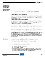
During asynchronous operation, the synchronization of the interrupt flags for the 
asynchronous timer takes three processor cycles plus one timer cycle. The timer is therefore 
advanced by at least one before the processor can read the timer value causing the setting 
of the interrupt flag. The output compare pin is changed on the timer clock and is not 
synchronized to the processor clock.

Timer/Counter 
Interrupt Mask 
Register – TIMSK

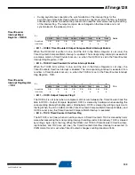
• Bit 1 – OCIE0: Timer/Counter0 Output Compare Match Interrupt Enable

When the OCIE0 bit is written to one, and the I-bit in the Status Register is set (one), the
Timer/Counter0 Compare Match interrupt is enabled. The corresponding interrupt is executed if
a compare match in Timer/Counter0 occurs, i.e., when the OCF0 bit is set in the Timer/Counter
Interrupt Flag Register – TIFR.

• Bit 0 – TOIE0: Timer/Counter0 Overflow Interrupt Enable

When the TOIE0 bit is written to one, and the I-bit in the Status Register is set (one), the
Timer/Counter0 Overflow interrupt is enabled. The corresponding interrupt is executed if an
overflow in Timer/Counter0 occurs, i.e., when the TOV0 bit is set in the Timer/Counter Interrupt
Flag Register – TIFR.

Timer/Counter 
Interrupt Flag Register 
– TIFR

• Bit 1 – OCF0: Output Compare Flag 0

The OCF0 bit is set (one) when a compare match occurs between the Timer/Counter0 and the
data in OCR0 – Output Compare Register0. OCF0 is cleared by hardware when executing the
corresponding interrupt handling vector. Alternatively, OCF0 is cleared by writing a logic one to
the flag. When the I-bit in SREG, OCIE0 (Timer/Counter0 Compare Match Interrupt Enable), and
OCF0 are set (one), the Timer/Counter0 Compare Match Interrupt is executed.

• Bit 0 – TOV0: Timer/Counter0 Overflow Flag

The bit TOV0 is set (one) when an overflow occurs in Timer/Counter0. TOV0 is cleared by hard-
ware when executing the corresponding interrupt handling vector. Alternatively, TOV0 is cleared
by writing a logic one to the flag. When the SREG I-bit, TOIE0 (Timer/Counter0 Overflow Inter-
rupt Enable), and TOV0 are set (one), the Timer/Counter0 Overflow Interrupt is executed. In
PWM mode, this bit is set when Timer/Counter0 changes counting direction at $00.

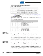
Bit

7

6

5

4

3

2

1

0

OCIE2

TOIE2

TICIE1

OCIE1A

OCIE1B

TOIE1

OCIE0

TOIE0

TIMSK

Read/Write

R/W

R/W

R/W

R/W

R/W

R/W

R/W

R/W

Initial Value

0

0

0

0

0

0

0

0

Bit

7

6

5

4

3

2

1

0

OCF2

TOV2

ICF1

OCF1A

OCF1B

TOV1

OCF0

TOV0

TIFR

Read/Write

R/W

R/W

R/W

R/W

R/W

R/W

R/W

R/W

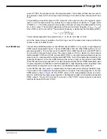
Initial  Value

0

0

0

0

0

0

0

0

Содержание ATmega128

Страница 1: ...escalers and Compare Modes Two Expanded 16 bit Timer Counters with Separate Prescaler Compare Mode and Capture Mode Real Time Counter with Separate Oscillator Two 8 bit PWM Channels 6 PWM Channels wit...

Страница 2: ...11 12 13 14 15 16 48 47 46 45 44 43 42 41 40 39 38 37 36 35 34 33 PEN RXD0 PDI PE0 TXD0 PDO PE1 XCK0 AIN0 PE2 OC3A AIN1 PE3 OC3B INT4 PE4 OC3C INT5 PE5 T3 INT6 PE6 ICP3 INT7 PE7 SS PB0 SCK PB1 MOSI P...

Страница 3: ...RTA DATA REGISTER PORTD TIMING AND CONTROL OSCILLATOR OSCILLATOR INTERRUPT UNIT EEPROM SPI USART0 STATUS REGISTER Z Y X ALU PORTB DRIVERS PORTE DRIVERS PORTA DRIVERS PORTF DRIVERS PORTD DRIVERS PORTC...

Страница 4: ...le memory technology The On chip ISP Flash allows the program memory to be reprogrammed in system through an SPI serial interface by a conventional nonvolatile memory programmer or by an On chip Boot...

Страница 5: ...errun comes earlier Unused I O bits in ATmega103 should be written to 0 to ensure same operation in ATmega128 Pin Descriptions VCC Digital supply voltage GND Ground Port A PA7 PA0 Port A is an 8 bit b...

Страница 6: ...l features of the ATmega128 as listed on page 81 Port F PF7 PF0 Port F serves as the analog inputs to the A D Converter Port F also serves as an 8 bit bi directional I O port if the A D Converter is n...

Страница 7: ...XTAL2 Output from the inverting Oscillator amplifier AVCC AVCC is the supply voltage pin for Port F and the A D Converter It should be externally con nected to VCC even if the ADC is not used If the...

Страница 8: ...eets are available for download on http www atmel com avr ATmega128 L rev A M characterization is found in the ATmega128 Appendix A Note 1 Data Retention Reliability Qualification results show that th...

Страница 9: ...compi lation Be aware that not all C compiler vendors include bit definitions in the header files and interrupt handling in C is compiler dependent Please confirm with the C compiler documentation fo...

Страница 10: ...c Unit ALU operation In a typ ical ALU operation two operands are output from the Register file the operation is executed and the result is stored back in the Register file in one clock cycle Six of t...

Страница 11: ...i tion The lower the interrupt vector address the higher the priority The I O memory space contains 64 addresses which can be accessed directly or as the Data Space locations following those of the Re...

Страница 12: ...n Bit S N V The S bit is always an exclusive or between the negative flag N and the two s complement over flow flag V See the Instruction Set Description for detailed information Bit 3 V Two s Complem...

Страница 13: ...R26 R31 have some added functions to their general purpose usage These reg isters are 16 bit address pointers for indirect addressing of the Data Space The three indirect address registers X Y and Z...

Страница 14: ...ementa tions of the AVR architecture is so small that only SPL is needed In this case the SPH Register will not be present RAM Page Z Select Register RAMPZ Bits 7 1 Res Reserved Bits These are reserve...

Страница 15: ...the section Memory Program ming on page 286 for details The lowest addresses in the program memory space are by default defined as the Reset and Interrupt vectors The complete list of vectors is show...

Страница 16: ...nterrupts do not necessarily have interrupt flags If the interrupt condition disappears before the interrupt is enabled the interrupt will not be triggered When the AVR exits from an interrupt it will...

Страница 17: ...a multi cycle instruction this instruction is completed before the interrupt is served If an interrupt occurs when the MCU is in Sleep mode the inter rupt execution response time is increased by four...

Страница 18: ...ogram section The Flash memory has an endurance of at least 10 000 write erase cycles The ATmega128 Program Counter PC is 16 bits wide thus addressing the 64K program memory locations The operation of...

Страница 19: ...rnal Memory are available in normal mode and 61440 Bytes in ATmega103 compatibility mode See External Memory Interface on page 26 for details on how to take advantage of the external memory map When t...

Страница 20: ...registers and the 4096 bytes of internal data SRAM in the ATmega128 are all accessible through all these addressing modes The Register file is described in General Purpose Register File on page 12 Fig...

Страница 21: ...ons must be taken In heavily filtered power supplies VCC is likely to rise or fall slowly on Power up down This causes the device for some period of time to run at a voltage lower than specified as mi...

Страница 22: ...EEPROM to be written When EEMWE is written to one writing EEWE to one within four clock cycles will write data to the EEPROM at the selected address If EEMWE is zero writing EEWE to one will have no e...

Страница 23: ...bit is cleared by hardware The user soft ware can poll this bit and wait for a zero before writing the next byte When EEWE has been set the CPU is halted for two cycles before the next instruction is...

Страница 24: ...ongoing SPM command to finish Assembly Code Example EEPROM_write Wait for completion of previous write sbic EECR EEWE rjmp EEPROM_write Set up address r18 r17 in address register out EEARH r18 out EEA...

Страница 25: ...ems using EEPROM and the same design solutions should be applied An EEPROM data corruption can be caused by two situations when the voltage is too low First a regular write sequence to the EEPROM requ...

Страница 26: ...is replaced with SRAM locations when the ATmega128 is in the ATmega103 compatibility mode For compatibility with future devices reserved bits should be written to zero if accessed Reserved I O memory...

Страница 27: ...ns in ATmega103 compatibility mode are Only two wait states settings are available SRW1n 0b00 and SRW1n 0b01 The number of bits that are assigned to address high byte are fixed The External Memory sec...

Страница 28: ...nal SRAM boundary is not mapped into the internal SRAM Figure 12 illustrates how to connect an external SRAM to the AVR using an octal latch typically 74 x 573 or equivalent which is transparent when...

Страница 29: ...e cannot exceed the time from the ALE pulse must be asserted low until data is stable during a read sequence See tLLRL tRLRH tDVRH in Tables 137 through Tables 144 on pages 328 330 The different wait...

Страница 30: ...SRWn1 SRW11 upper sector or SRW01 lower sector SRWn0 SRW10 upper sector or SRW00 lower sector The ALE pulse in period T6 is only present if the next instruction accesses the RAM internal or external...

Страница 31: ...te Select Bit For a detailed description in non ATmega103 compatibility mode see common description for the SRWn bits below XMCRA description In ATmega103 compatibility mode writing SRW10 to one enabl...

Страница 32: ...Table 4 Note 1 n 0 or 1 lower upper sector For further details of the timing and wait states of the External Memory Interface see Figures 13 through Figures 16 for how the setting of the SRW bits affe...

Страница 33: ...ing the first 4 352 bytes of data space It may appear that the first 4 352 bytes of the external memory are inaccessible external memory addresses 0x0000 to 0x10FF However when connecting an external...

Страница 34: ...ess Map with 32 KB External Memory 0x0000 0x10FF 0xFFFF 0x1100 0x7FFF 0x8000 0x90FF 0x9100 0x0000 0x10FF 0x1100 0x7FFF Memory Configuration A Memory Configuration B Internal Memory Unused AVR Memory M...

Страница 35: ...the following code examples Note 1 See About Code Examples on page 9 Care must be exercised using this option as most of the memory is masked away Assembly Code Example 1 OFFSET is defined to 0x2000 t...

Страница 36: ...ions I O Clock clkI O The I O clock is used by the majority of the I O modules like Timer Counters SPI and USART The I O clock is also used by the External Interrupt module but note that some external...

Страница 37: ...the XDIVEN bit is set one If the value of these bits is denoted d the following formula defines the resulting CPU and peripherals clock frequency fCLK The value of these bits can only be changed when...

Страница 38: ...cillator cycles used for each time out is shown in Table 7 The frequency of the Watchdog Oscillator is voltage dependent as shown in the Typical Char acteristics on page 333 Default Clock Source The d...

Страница 39: ...16 MHz with CKOPT programmed C1 and C2 should always be equal for both crystals and resonators The optimal value of the capacitors depends on the crystal or resonator in use the amount of stray capac...

Страница 40: ...value of 36 pF When this Oscillator is selected start up times are determined by the SUT fuses as shown in Table 10 Note 1 These options should only be used if frequency stability at start up is not...

Страница 41: ...t modes each optimized for a specific frequency range The operating mode is selected by the fuses CKSEL3 0 as shown in Table 11 When this Oscillator is selected start up times are determined by the SU...

Страница 42: ...ice is shipped with this option selected Oscillator Calibration Register OSCCAL Note OSCCAL Register is not available in ATmega103 compatibility mode Bits 7 0 CAL7 0 Oscillator Calibration Value Writi...

Страница 43: ...Drive Configuration When this clock source is selected start up times are determined by the SUT fuses as shown in Table 16 When applying an external clock it is required to avoid sudden changes in th...

Страница 44: ...rectly between the pins No external capacitors are needed The Oscillator is opti mized for use with a 32 768 kHz watch crystal Applying an external clock source to TOSC1 is not recommended Note The Ti...

Страница 45: ...and executes from the Reset Vector Figure 18 on page 36 presents the different clock systems in the ATmega128 and their distribu tion The figure is helpful in selecting an appropriate sleep mode MCU C...

Страница 46: ...bits are written to 010 the SLEEP instruction makes the MCU enter Power down mode In this mode the External Oscillator is stopped while the External Interrupts the Two wire Serial Interface address w...

Страница 47: ...to Power save mode with the exception that the Oscillator is kept running From Extended Standby mode the device wakes up in six clock cycles Notes 1 External Crystal or resonator selected as clock sou...

Страница 48: ...sleep modes this will contribute significantly to the total current consumption Refer to Brown out Detector on page 48 for details on how to configure the Brown out Detector Internal Voltage Referenc...

Страница 49: ...ways to avoid this Disable OCDEN Fuse Disable JTAGEN Fuse Write one to the JTD bit in MCUCSR The TDO pin is left floating when the JTAG interface is enabled while the JTAG TAP controller is not shift...

Страница 50: ...all reset sources have gone inactive a delay counter is invoked stretching the internal reset This allows the power to reach a stable level before normal operation starts The time out period of the de...

Страница 51: ...lse width on RESET Pin 1 5 s VBOT Brown out Reset Threshold Voltage 2 BODLEVEL 1 2 4 2 6 2 9 V BODLEVEL 0 3 7 4 0 4 5 tBOD Minimum low voltage period for Brown out Detection BODLEVEL 1 2 s BODLEVEL 0...

Страница 52: ...a failure in supply voltage A Power on Reset POR circuit ensures that the device is reset from Power on Reaching the Power on Reset threshold voltage invokes the delay counter which determines how lo...

Страница 53: ...detection level should be interpreted as VBOT VBOT VHYST 2 and VBOT VBOT VHYST 2 The BOD circuit can be enabled disabled by the fuse BODEN When the BOD is enabled BODEN programmed and VCC decreases to...

Страница 54: ...flag Bit 2 BORF Brown out Reset Flag This bit is set if a Brown out Reset occurs The bit is reset by a Power on Reset or by writing a logic zero to the flag Bit 1 EXTRF External Reset Flag This bit i...

Страница 55: ...ation data for typical values at other VCC levels By controlling the Watchdog Timer prescaler the Watchdog Reset interval can be adjusted as shown in Table 22 on page 57 The WDR Watchdog Reset instruc...

Страница 56: ...chdog Enable When the WDE is written to logic one the Watchdog Timer is enabled and if the WDE is written to logic zero the Watchdog Timer function is disabled WDE can only be cleared if the WDCE bit...

Страница 57: ...s 2 0 WDP2 WDP1 WDP0 Watchdog Timer Prescaler 2 1 and 0 The WDP2 WDP1 and WDP0 bits determine the Watchdog Timer prescaling when the Watch dog Timer is enabled The different prescaling values and thei...

Страница 58: ...led but can be enabled by writing the WDE bit to 1 without any restriction A timed sequence is needed when changing the Watchdog Time out period or disabling an enabled Watchdog Timer To disable an en...

Страница 59: ...to WDCE and WDE Even though the WDE always is set the WDE must be written to one to start the timed sequence 2 Within the next four clock cycles in the same operation write the WDP bits as desired but...

Страница 60: ...equest 7 10 0012 TIMER2 COMP Timer Counter2 Compare Match 11 0014 TIMER2 OVF Timer Counter2 Overflow 12 0016 TIMER1 CAPT Timer Counter1 Capture Event 13 0018 TIMER1 COMPA Timer Counter1 Compare Match...

Страница 61: ...vectors are not used and regular program code can be placed at these locations This is also the case if the Reset Vector is in the Application section while the interrupt vectors are in the Boot secti...

Страница 62: ...2 jmp SPI_STC SPI Transfer Complete Handler 0024 jmp USART0_RXC USART0 RX Complete Handler 0026 jmp USART0_DRE USART0 UDR Empty Handler 0028 jmp USART0_TXC USART0 TX Complete Handler 002A jmp ADC ADC...

Страница 63: ...the Reset and Interrupt Vector Addresses is Address LabelsCode Comments org 0002 0002 jmp EXT_INT0 IRQ0 Handler 0004 jmp EXT_INT1 IRQ1 Handler 0044 jmp SPM_RDY Store Program Memory Ready Handler org F...

Страница 64: ...ctor Change Enable IVCE bit to one 2 Within four cycles write the desired value to IVSEL while writing a zero to IVCE Interrupts will automatically be disabled while this sequence is executed Interrup...

Страница 65: ...en Setting the IVCE bit will disable interrupts as explained in the IVSEL description above See Code Example below Assembly Code Example Move_interrupts Enable change of interrupt vectors ldi r16 1 IV...

Страница 66: ...the bit number However when using the register or bit defines in a program the precise form must be used For example PORTB3 for bit no 3 in Port B here documented generally as PORTxn The physical I O...

Страница 67: ...ero Pxn is configured as an input pin If PORTxn is written logic one when the pin is configured as an input pin the pull up resistor is activated To switch the pull up resistor off PORTxn has to be wr...

Страница 68: ...ding latch consti tute a synchronizer This is needed to avoid metastability if the physical pin changes value near the edge of the internal clock but it also introduces a delay Figure 31 shows a timin...

Страница 69: ...between and 1 system clock period depending upon the time of assertion When reading back a software assigned pin value a nop instruction must be inserted as indi cated in Figure 32 The out instructio...

Страница 70: ...ating or have an analog signal level close to VCC 2 SLEEP is overridden for port pins enabled as External Interrupt pins If the External Interrupt Request is not enabled SLEEP is active also for these...

Страница 71: ...e 30 can be overridden by alternate functions The overriding signals may not be present in all port pins but the figure serves as a generic description applicable to all port pins in the AVR microcont...

Страница 72: ...ue If DDOE is set the Output Driver is enabled disabled when DDOV is set cleared regardless of the setting of the DDxn Register bit PVOE Port Value Override Enable If this signal is set and the Output...

Страница 73: ...R W R W R W Initial Value 0 0 0 0 0 0 0 0 Table 27 Port A Pins Alternate Functions Port Pin Alternate Function PA7 AD7 External memory interface address and data bit 7 PA6 AD6 External memory interfa...

Страница 74: ...function Table 29 Overriding Signals for Alternate Functions in PA3 PA0 Signal Name PA3 AD3 PA2 AD2 PA1 AD1 PA0 AD0 PUOE SRE SRE SRE SRE PUOV WR ADA PORTA3 PUD WR ADA PORTA2 PUD WR ADA PORTA1 PUD WR...

Страница 75: ...ntrolled by the PORTB3 bit MOSI Port B Bit 2 MOSI SPI Master Data output Slave Data input for SPI channel When the SPI is enabled as a slave this pin is configured as an input regardless of the settin...

Страница 76: ...NABLE 1 OC1B ENABLE OC1A ENABLE OC0 ENABLE PVOV OC2 OC1C 1 OC1B OC1A OC0B DIEOE 0 0 0 0 DIEOV 0 0 0 0 DI AIO Table 32 Overriding Signals for Alternate Functions in PB3 PB0 Signal Name PB3 MISO PB2 MOS...

Страница 77: ...erface Table 34 and Table 35 relate the alternate functions of Port C to the overriding signals shown in Figure 33 on page 71 Note 1 XMM 0 in ATmega103 compatibility mode Table 33 Port C Pins Alternat...

Страница 78: ...us mode Table 35 Overriding Signals for Alternate Functions in PC3 PC0 1 Signal Name PC3 A11 PC2 A10 PC1 A9 PC0 A8 PUOE SRE XMM 5 SRE XMM 6 SRE XMM 7 SRE XMM 7 PUOV 0 0 0 0 DDOE SRE XMM 5 SRE XMM 6 SR...

Страница 79: ...nal interrupt source to the MCU SDA Two wire Serial Interface Data When the TWEN bit in TWCR is set one to enable the Two wire Serial Interface pin PD1 is disconnected from the port and becomes the Se...

Страница 80: ...PUOE 0 0 0 0 PUOV 0 0 0 0 DDOE 0 0 0 0 DDOV 0 0 0 0 PVOE 0 0 UMSEL1 0 PVOV 0 0 XCK1 OUTPUT 0 DIEOE 0 0 0 0 DIEOV 0 0 0 0 DI T2 INPUT T1 INPUT XCK1 INPUT ICP1 INPUT AIO Table 38 Overriding Signals for...

Страница 81: ...ed as an output DDE4 set one to serve this function The OC3B pin is also the output pin for the PWM mode timer function AIN1 OC3A Port E Bit 3 AIN1 Analog Comparator Negative input This pin is directl...

Страница 82: ...ART0 Receive Pin Receive Data Data input pin for the USART0 When the USART0 receiver is enabled this pin is configured as an input regardless of the value of DDRE0 When the USART0 forces this pin to b...

Страница 83: ...a Out Serial output data from Instruction Register or Data Register When the JTAG interface is enabled this pin can not be used as an I O pin The TDO pin is tri stated unless TAP states that shift out...

Страница 84: ...nel 3 0 Table 43 Overriding Signals for Alternate Functions in PF7 PF4 Signal Name PF7 ADC7 TDI PF6 ADC6 TDO PF5 ADC5 TMS PF4 ADC4 TCK PUOE JTAGEN JTAGEN JTAGEN JTAGEN PUOV 1 0 1 1 DDOE JTAGEN JTAGEN...

Страница 85: ...tor amplifier In this mode a Crystal Oscillator is connected to this pin and the pin can not be used as an I O pin ALE Port G Bit 2 ALE is the external data memory Address Latch Enable signal RD Port...

Страница 86: ...86 2467S AVR 07 09 ATmega128 Table 47 Overriding Signals for Alternate Functions in PG0 Signal Name PG0 WR PUOE SRE PUOV 0 DDOE SRE DDOV 1 PVOE SRE PVOV WR DIEOE 0 DIEOV 0 DI AIO...

Страница 87: ...A5 PINA4 PINA3 PINA2 PINA1 PINA0 PINA Read Write R R R R R R R R Initial Value N A N A N A N A N A N A N A N A Bit 7 6 5 4 3 2 1 0 PORTB7 PORTB6 PORTB5 PORTB4 PORTB3 PORTB2 PORTB1 PORTB0 PORTB Read Wr...

Страница 88: ...PORTD3 PORTD2 PORTD1 PORTD0 PORTD Read Write R W R W R W R W R W R W R W R W Initial Value 0 0 0 0 0 0 0 0 Bit 7 6 5 4 3 2 1 0 DDD7 DDD6 DDD5 DDD4 DDD3 DDD2 DDD1 DDD0 DDRD Read Write R W R W R W R W...

Страница 89: ...TOSC1 TOSC2 WR RD and ALE Bit 7 6 5 4 3 2 1 0 DDF7 DDF6 DDF5 DDF4 DDF3 DDF2 DDF1 DDF0 DDRF Read Write R W R W R W R W R W R W R W R W Initial Value 0 0 0 0 0 0 0 0 Bit 7 6 5 4 3 2 1 0 PINF7 PINF6 PINF...

Страница 90: ...d by the SUT fuses as described in Clock Systems and their Distribution on page 36 If the level is sampled twice by the Watchdog Oscillator clock but disappears before the end of the start up time the...

Страница 91: ...rate an interrupt If enabled a level triggered interrupt will generate an interrupt request as long as the pin is held low Note 1 n 7 6 5 or 4 When changing the ISCn1 ISCn0 bits the interrupt must be...

Страница 92: ...iggers an interrupt request INTF7 0 becomes set one If the I bit in SREG and the corresponding interrupt enable bit INT7 0 in EIMSK are set one the MCU will jump to the interrupt vector The flag is cl...

Страница 93: ...r Counter Block Diagram Registers The Timer Counter TCNT0 and Output Compare Register OCR0 are 8 bit registers Interrupt request shorten as Int Req signals are all visible in the Timer Interrupt Flag...

Страница 94: ...by an internal synchronous or an external asynchronous clock source The clock source clkT0 is by default equal to the MCU clock clkI O When the AS0 bit in the ASSR Register is written to logic one th...

Страница 95: ...forms are generated on the output compare output OC0 For more details about advanced counting sequences and waveform generation see Modes of Operation on page 98 The Timer Counter overflow TOV0 flag i...

Страница 96: ...are match had occurred the COM01 0 bits settings define whether the OC0 pin is set cleared or toggled Compare Match Blocking by TCNT0 Write All CPU write operations to the TCNT0 Register will block an...

Страница 97: ...the OC0 pin direction input or output is still controlled by the Data Direction Register DDR for the port pin The Data Direction Regis ter bit for the OC0 pin DDR_OC0 must be set as output before the...

Страница 98: ...n be increased by software There are no special cases to consider in the normal mode a new counter value can be written anytime The output compare unit can be used to generate interrupts at some given...

Страница 99: ...PWM option by its sin gle slope operation The counter counts from BOTTOM to MAX then restarts from BOTTOM In non inverting Compare Output mode the output compare OC0 is cleared on the compare match b...

Страница 100: ...equency for the output can be calculated by the following equation The N variable represents the prescale factor 1 8 32 64 128 256 or 1024 The extreme values for the OCR0 Register represent special ca...

Страница 101: ...phase correct PWM mode is shown on Figure 40 The TCNT0 value is in the timing diagram shown as a histogram for illustrating the dual slope operation The diagram includes non inverted and inverted PWM...

Страница 102: ...ting Compare Match The timer starts counting from a higher value than the one in OCR0 and for that reason misses the Compare Match and hence the OCn change that would have happened on the way up Timer...

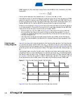
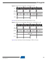
Страница 103: ...f OCF0 in all modes except CTC mode Figure 43 Timer Counter Timing Diagram Setting of OCF0 with Prescaler fclk_I O 8 Figure 44 shows the setting of OCF0 and the clearing of TCNT0 in CTC mode TOVn TCNT...

Страница 104: ...a strobe Therefore it is the value present in the COM01 0 bits that determines the effect of the forced compare A FOC0 strobe will not generate any interrupt nor will it clear the timer in CTC mode us...

Страница 105: ...e set to fast PWM mode Note 1 A special case occurs when OCR0 equals TOP and COM01 is set In this case the compare match is ignored but the set or clear is done at BOTTOM See Fast PWM Mode on page 99...

Страница 106: ...t is continuously compared with the counter value TCNT0 A match can be used to generate an output compare interrupt or to generate a waveform output on the OC0 pin Table 55 Compare Output Mode Phase C...

Страница 107: ...this bit is cleared by hard ware A logical zero in this bit indicates that TCCR0 is ready to be updated with a new value If a write is performed to any of the three Timer Counter0 Registers while its...

Страница 108: ...esponding Update Busy flag in ASSR returns to zero 3 Enter Power save or Extended Standby mode When the asynchronous operation is selected the 32 768 kHZ Oscillator for Timer Counter0 is always runnin...

Страница 109: ...in the Timer Counter Interrupt Flag Register TIFR Timer Counter Interrupt Flag Register TIFR Bit 1 OCF0 Output Compare Flag 0 The OCF0 bit is set one when a compare match occurs between the Timer Coun...

Страница 110: ...0 stop may be selected Setting the PSR0 bit in SFIOR resets the prescaler This allows the user to operate with a predictable prescaler Special Function IO Register SFIOR Bit 7 TSM Timer Counter Synch...

Страница 111: ...the Timer Counter0 prescaler will be reset This bit is normally cleared immediately by hardware If this bit is written when Timer Counter0 is operating in asynchronous mode the bit will remain one unt...

Страница 112: ...at in ATmega103 compatibility mode only one 16 bit Timer Counter is available Timer Counter1 Also note that in ATmega103 compatibility mode the Timer Counter1 has two Compare Registers Compare A and C...

Страница 113: ...not shown in the figure since these registers are shared by other timer units The Timer Counter can be clocked internally via the prescaler or by an external clock source on the Tn pin The Clock Sele...

Страница 114: ...imer Counter This 16 bit Timer Counter is fully compatible with the earlier version regarding All 16 bit Timer Counter related I O register address locations including timer interrupt registers Bit lo...

Страница 115: ...he high byte must be written before the low byte For a 16 bit read the low byte must be read before the high byte The following code examples show how to access the 16 bit timer registers assuming tha...

Страница 116: ...the TCNTn value in the r17 r16 register pair Assembly Code Example 1 TIM16_ReadTCNTn Save global interrupt flag in r18 SREG Disable interrupts cli Read TCNTn into r17 r16 in r16 TCNTnL in r17 TCNTnH R...

Страница 117: ...ter where the high byte is the same for all registers written then the high byte only needs to be written once However note that the same rule of atomic operation described previously also applies in...

Страница 118: ...the high byte Temporary Register TEMP The Temporary Register is updated with the TCNTnH value when the TCNTnL is read and TCNTnH is updated with the Temporary Register value when TCNTnL is written Thi...

Страница 119: ...bit names indicates the Timer Counter number Figure 48 Input Capture Unit Block Diagram Note The Analog Comparator Output ACO can only trigger the Timer Counter1 ICP not Timer Counter3 When a change...

Страница 120: ...ICPn pin Noise Canceler The noise canceler improves noise immunity by using a simple digital filtering scheme The noise canceler input is monitored over four samples and all four must be equal for ch...

Страница 121: ...lution In addition to the counter resolution the TOP value defines the period time for waveforms generated by the waveform generator Figure 49 shows a block diagram of the output compare unit The smal...

Страница 122: ...clear the timer but the OCnx pin will be updated as if a real compare match had occurred the COMnx1 0 bits settings define whether the OCnx pin is set cleared or toggled Compare Match Blocking by TCNT...

Страница 123: ...fore the OCnx value is visible on the pin The port override function is generally independent of the waveform generation mode but there are some exceptions Refer to Table 58 Table 59 and Table 60 for...

Страница 124: ...er resolution can be increased by soft ware There are no special cases to consider in the normal mode a new counter value can be written anytime The Input Capture unit is easy to use in normal mode Ho...

Страница 125: ...requency PWM waveform generation option The fast PWM differs from the other PWM options by its single slope operation The counter counts from BOTTOM to TOP then restarts from BOTTOM In non inverting C...

Страница 126: ...OCRnA Register however is double buffered This feature allows the OCRnA I O location to be written anytime When the OCRnA I O location is written the value written will be put into the OCRnA buffer R...

Страница 127: ...utput mode the output compare OCnx is cleared on the compare match between TCNTn and OCRnx while counting up and set on the compare match while downcounting In inverting Output Compare mode the operat...

Страница 128: ...at TOP This implies that the length of the falling slope is determined by the previous TOP value while the length of the rising slope is determined by the new TOP value When these two values differ th...

Страница 129: ...operation gives a lower maximum operation fre quency compared to the single slope operation However due to the symmetric feature of the dual slope PWM modes these modes are preferred for motor contro...

Страница 130: ...alues By using ICRn the OCRnA Register is free to be used for generating a PWM output on OCnA However if the base PWM frequency is actively changed by changing the TOP value using the OCRnA as TOP is...

Страница 131: ...nter is a synchronous design and the timer clock clkTn is therefore shown as a clock enable signal in the following figures The figures include information on when interrupt flags are set and when the...

Страница 132: ...mer Counter Timing Diagram no Prescaling Figure 58 shows the same timing data but with the prescaler enabled Figure 58 Timer Counter Timing Diagram with Prescaler fclk_I O 8 TOVn FPWM and ICFn if used...

Страница 133: ...n it is connected to How ever note that the Data Direction Register DDR bit corresponding to the OCnA OCnB or OCnC pin must be set in order to enable the output driver When the OCnA OCnB or OCnC is co...

Страница 134: ...CnB OCnC disconnected 0 1 WGMn3 0 15 Toggle OCnA on Compare Match OCnB OCnC disconnected normal port operation For all other WGMn settings normal port operation OCnA OCnB OCnC disconnected 1 0 Clear O...

Страница 135: ...he timer Table 61 Waveform Generation Mode Bit Description Mode WGMn3 WGMn2 CTCn WGMn1 PWMn1 WGMn0 PWMn0 Timer Counter Mode of Operation 1 TOP Update of OCRnx at TOVn Flag Set on 0 0 0 0 0 Normal 0xFF...

Страница 136: ...the ICESn setting the counter value is copied into the Input Capture Register ICRn The event will also set the Input Capture Flag ICFn and this can be used to cause an Input Capture Interrupt if this...

Страница 137: ...ue present in the COMnx1 0 bits that determine the effect of the forced compare A FOCnA FOCnB FOCnC strobe will not generate any interrupt nor will it clear the timer in Clear Timer on Compare Match C...

Страница 138: ...ing timer clock for all compare units Output Compare Register 1 A OCR1AH and OCR1AL Output Compare Register 1 B OCR1BH and OCR1BL Output Compare Register 1 C OCR1CH and OCR1CL Output Compare Register...

Страница 139: ...e Register is 16 bit in size To ensure that both the high and low bytes are read simultaneously when the CPU accesses these registers the access is performed using an 8 bit temporary High Byte Registe...

Страница 140: ...n page 60 is executed when the TOV1 flag located in TIFR is set Extended Timer Counter Interrupt Mask Register ETIMSK Note This register is not available in ATmega103 compatibility mode Bit 7 6 Reserv...

Страница 141: ...curs on the ICP1 pin When the Input Capture Register ICR1 is set by the WGMn3 0 to be used as the TOP value the ICF1 flag is set when the coun ter reaches the TOP value ICF1 is automatically cleared w...

Страница 142: ...set in the timer clock cycle after the counter TCNT3 value matches the Output Compare Register B OCR3B Note that a forced output compare FOC3B strobe will not set the OCF3B flag OCF3B is automaticall...

Страница 143: ...a forced output compare FOC1C strobe will not set the OCF1C flag OCF1C is automatically cleared when the Output Compare Match 1 C interrupt vector is exe cuted Alternatively OCF1C can be cleared by w...

Страница 144: ...clock cycles where N equals the prescaler divisor 8 64 256 or 1024 It is possible to use the Prescaler Reset for synchronizing the Timer Counter to program execu tion However care must be taken if th...

Страница 145: ...chronization mode In this mode the value that is written to the PSR0 and PSR321 bits is kept hence keeping the corresponding prescaler reset signals asserted This ensures that the corresponding Timer...

Страница 146: ...er Counter Block Diagram Registers The Timer Counter TCNT2 and Output Compare Register OCR2 are 8 bit registers Interrupt request abbreviated to Int Req in the figure signals are all visible in the Ti...

Страница 147: ...the clock select CS22 0 bits located in the Timer Counter Control Register TCCR2 For details on clock sources and prescaler see Timer Counter3 Timer Counter2 and Timer Counter1 Prescalers on page 144...

Страница 148: ...PU interrupt Output Compare Unit The 8 bit comparator continuously compares TCNT2 with the Output Compare Register OCR2 Whenever TCNT2 equals OCR2 the comparator signals a match A match will set the o...

Страница 149: ...re matches for one timer clock cycle there are risks involved when changing TCNT2 when using the output compare channel independently of whether the Timer Counter is running or not If the value writte...

Страница 150: ...n page 158 For fast PWM mode refer to Table 66 on page 158 and for phase correct PWM refer to Table 67 on page 158 A change of the COM21 0 bits state will have effect at the first compare match after...

Страница 151: ...ng external events The timing diagram for the CTC mode is shown in Figure 65 The counter value TCNT2 increases until a compare match occurs between TCNT2 and OCR2 and then counter TCNT2 is cleared Fig...

Страница 152: ...the counter value matches the MAX value The counter is then cleared at the following timer clock cycle The timing diagram for the fast PWM mode is shown in Figure 66 The TCNT2 value is in the timing...

Страница 153: ...generation option The phase correct PWM mode is based on a dual slope operation The counter counts repeatedly from BOTTOM to MAX and then from MAX to BOTTOM In non inverting Compare Output mode the o...

Страница 154: ...ect PWM can be calculated by the follow ing equation The N variable represents the prescale factor 1 8 64 256 or 1024 The extreme values for the OCR2 Register represent special cases when generating a...

Страница 155: ...lude information on when interrupt flags are set Figure 68 contains timing data for basic Timer Counter operation The figure shows the count sequence close to the MAX value in all modes other than pha...

Страница 156: ...e 71 shows the setting of OCF2 and the clearing of TCNT2 in CTC mode Figure 71 Timer Counter Timing Diagram Clear Timer on Compare Match Mode with Pres caler fclk_I O 8 OCFn OCRn TCNTn OCRn Value OCRn...

Страница 157: ...match CTC mode and two types of Pulse Width Modulation PWM modes See Table 64 and Modes of Operation on page 150 Note The CTC2 and PWM2 bit definition names are now obsolete Use the WGM21 0 definitio...

Страница 158: ...Mode COM21 COM20 Description 0 0 Normal port operation OC2 disconnected 0 1 Toggle OC2 on compare match 1 0 Clear OC2 on compare match 1 1 Set OC2 on compare match Table 66 Compare Output Mode Fast P...

Страница 159: ...one and the I bit in the Status Register is set one the Timer Counter2 Compare Match interrupt is enabled The corresponding interrupt is executed if a compare match in Timer Counter2 occurs i e when...

Страница 160: ...ne the Timer Counter2 Compare Match Interrupt is executed Bit 6 TOV2 Timer Counter2 Overflow Flag The bit TOV2 is set one when an overflow occurs in Timer Counter2 TOV2 is cleared by hard ware when ex...

Страница 161: ...hannels are modulated together as shown in the block diagram Figure 72 Description The Output Compare unit 1C and Output Compare unit 2 shares the PB7 port pin for output The outputs of the Output Com...

Страница 162: ...gram In this example Timer Counter2 provides the carrier while the modulating signal is generated by the Output Compare unit C of the Timer Counter1 The resolution of the PWM signal OC1C is reduced by...

Страница 163: ...re 1 on page 2 and Table 30 on page 74 for SPI pin placement The interconnection between Master and Slave CPUs with SPI is shown in Figure 76 The sys tem consists of two Shift Registers and a Master c...

Страница 164: ...upt enable bit SPIE in the SPCR Register is set an interrupt is requested The Slave may continue to place new data to be sent into SPDR before reading the incoming data The last incoming byte will be...

Страница 165: ...e DD_MOSI with DDB5 and DDR_SPI with DDRB Note 1 See About Code Examples on page 9 Assembly Code Example 1 SPI_MasterInit Set MOSI and SCK output all others input ldi r17 1 DD_MOSI 1 DD_SCK out DDR_SP...

Страница 166: ...others input ldi r17 1 DD_MISO out DDR_SPI r17 Enable SPI ldi r17 1 SPE out SPCR r17 ret SPI_SlaveReceive Wait for reception complete sbis SPSR SPIF rjmp SPI_SlaveReceive Read received data and retur...

Страница 167: ...a slave and starting to send data to it To avoid bus contention the SPI system takes the following actions 1 The MSTR bit in SPCR is cleared and the SPI system becomes a slave As a result of the SPI...

Страница 168: ...gure 78 for an example The CPHA func tionality is summarized below Bits 1 0 SPR1 SPR0 SPI Clock Rate Select 1 and 0 These two bits control the SCK rate of the device configured as a master SPR1 and SP...

Страница 169: ...bits are reserved bits in the ATmega128 and will always read as zero Bit 0 SPI2X Double SPI Speed Bit When this bit is written logic one the SPI speed SCK Frequency will be doubled when the SPI is in...

Страница 170: ...sfer Format with CPHA 1 Table 73 CPOL and CPHA Functionality Leading edge Trailing edge SPI mode CPOL 0 CPHA 0 Sample Rising Setup Falling 0 CPOL 0 CPHA 1 Setup Rising Sample Falling 1 CPOL 1 CPHA 0 S...

Страница 171: ...Includes False Start Bit Detection and Digital Low Pass Filter Three Separate Interrupts on TX Complete TX Data Register Empty and RX Complete Multi processor Communication Mode Double Speed Asynchron...

Страница 172: ...logic for handling different serial frame formats The write buffer allows a continuous transfer of data without any delay between frames The Receiver is the most complex part of the USART module due...

Страница 173: ...until a new start bit is detected The USART is therefore more resistant to Data OverRun DOR error conditions The following control bits have changed name but have same functionality and register locat...

Страница 174: ...equations for calculating the baud rate in bits per second and for calculating the UBRR value for each mode of operation using an internally generated clock source Note 1 The baud rate is defined to b...

Страница 175: ...recommended to add some margin to avoid possible loss of data due to frequency variations Synchronous Clock Operation When Synchronous mode is used UMSEL 1 the XCK pin will be used as either clock inp...

Страница 176: ...RxD or TxD An IDLE line must be high The frame format used by the USART is set by the UCSZ2 0 UPM1 0 and USBS bits in UCSRB and UCSRC The receiver and transmitter use the same setting Note that changi...

Страница 177: ...y The examples assume asynchronous operation using polling no interrupts enabled and a fixed frame format The baud rate is given as a function parameter For the assembly code the baud rate parameter i...

Страница 178: ...st stop bit of the previous frame is transmitted When the Shift Register is loaded with new data it will transfer one complete frame at the rate given by the baud register U2X bit or by XCK depending...

Страница 179: ...o flags that indicate its state USART Data Register Empty UDRE and Transmit Complete TXC Both flags can be used for generating interrupts The Data Register Empty UDRE flag indicates whether the transm...

Страница 180: ...he transmitter control logic inserts the parity bit between the last data bit and the first stop bit of the frame that is sent Disabling the Transmitter The disabling of the Transmitter setting the TX...

Страница 181: ...unction can be used Note 1 See About Code Examples on page 9 The function simply waits for data to be present in the receive buffer by checking the RXC flag before reading the buffer and returning the...

Страница 182: ...andles both nine bit characters and the status bits Assembly Code Example 1 USART_Receive Wait for data to be received sbis UCSRA RXC rjmp USART_Receive Get status and 9th bit then data from buffer in...

Страница 183: ...read location Another equality for the error flags is that they can not be altered by software doing a write to the flag location However all flags must be set to zero when the UCSRA is written for u...

Страница 184: ...receiver buffer FIFO will be flushed when the receiver is disabled Remaining data in the buffer will be lost Flushing the Receive Buffer The receiver buffer FIFO will be flushed when the receiver is d...

Страница 185: ...nization process is repeated for each start bit Asynchronous Data Recovery When the receiver clock is synchronized to the start bit the data recovery can begin The data recovery unit uses a state mach...

Страница 186: ...ated baud rate of the receiver does not have a similar see Table 75 base frequency the Receiver will not be able to synchronize the frames to the start bit The following equations can be used to calcu...

Страница 187: ...o be handled by the CPU in a system with multiple MCUs that communicate via the same serial bus The transmitter is unaffected by the MPCM setting but has to be used differently when it is a part of a...

Страница 188: ...ill be set as normal 3 Each slave MCU reads the UDR Register and determines if it has been selected If so it clears the MPCM bit in UCSRA otherwise it waits for the next address byte and keeps the MPC...

Страница 189: ...FIFO USART Control and Status Register A UCSRnA Bit 7 RXCn USART Receive Complete This flag bit is set when there are unread data in the receive buffer and cleared when the receive buffer is empty i e...

Страница 190: ...de When the MPCMn bit is written to one all the incoming frames received by the USART Receiver that do not contain address infor mation will be ignored The transmitter is unaffected by the MPCMn setti...

Страница 191: ...9 data bits Must be written before writing the low bits to UDRn USART Control and Status Register C UCSRnC Note that this register is not available in ATmega103 compatibility mode Bit 7 Reserved Bit T...

Страница 192: ...mple and the synchronous clock XCKn USART Baud Rate Registers UBRRnL and UBRRnH UBRRnH is not available in mega103 compatibility mode Table 79 USBSn Bit Settings USBSn Stop Bit s 0 1 bit 1 2 bits Tabl...

Страница 193: ...n11 0 USARTn Baud Rate Register This is a 12 bit register which contains the USARTn baud rate The UBRRnH contains the four most significant bits and the UBRRnL contains the eight least significant bit...

Страница 194: ...ateClosest Match BaudRate 1 100 Table 82 Examples of UBRR Settings for Commonly Used Oscillator Frequencies Baud Rate bps fosc 1 0000 MHz fosc 1 8432 MHz fosc 2 0000 MHz U2X 0 U2X 1 U2X 0 U2X 1 U2X 0...

Страница 195: ...600 23 0 0 47 0 0 25 0 2 51 0 2 47 0 0 95 0 0 14 4k 15 0 0 31 0 0 16 2 1 34 0 8 31 0 0 63 0 0 19 2k 11 0 0 23 0 0 12 0 2 25 0 2 23 0 0 47 0 0 28 8k 7 0 0 15 0 0 8 3 5 16 2 1 15 0 0 31 0 0 38 4k 5 0 0...

Страница 196: ...0 2 71 0 0 143 0 0 95 0 0 191 0 0 14 4k 34 0 8 68 0 6 47 0 0 95 0 0 63 0 0 127 0 0 19 2k 25 0 2 51 0 2 35 0 0 71 0 0 47 0 0 95 0 0 28 8k 16 2 1 34 0 8 23 0 0 47 0 0 31 0 0 63 0 0 38 4k 12 0 2 25 0 2...

Страница 197: ...0 U2X 1 UBRR Error UBRR Error 2400 416 0 1 832 0 0 4800 207 0 2 416 0 1 9600 103 0 2 207 0 2 14 4k 68 0 6 138 0 1 19 2k 51 0 2 103 0 2 28 8k 34 0 8 68 0 6 38 4k 25 0 2 51 0 2 57 6k 16 2 1 34 0 8 76 8k...

Страница 198: ...e pull up resistor for each of the TWI bus lines All devices connected to the bus have individual addresses and mechanisms for resolving bus contention are inherent in the TWI protocol Figure 86 TWI B...

Страница 199: ...onditions The master initiates and terminates a data transmission The transmission is initiated when the master issues a START condition on the bus and it is terminated when the master issues a STOP c...

Страница 200: ...t the same message to several slaves in the system When the general call address followed by a Write bit is transmitted on the bus all slaves set up to acknowledge the general call will pull the SDA l...

Страница 201: ...TWI protocol allows bus systems with several masters Special concerns have been taken in order to ensure that transmissions will proceed as normal even if two or more masters initiate a transmission...

Страница 202: ...ne does not match the value the master had output it has lost the arbitration Note that a master can only lose arbitration when it outputs a high SDA value while another master outputs a low value The...

Страница 203: ...STOP condition It is the user software s responsibility to ensure that these illegal arbitration conditions never occur This implies that in multi master systems all data transfers must use the same...

Страница 204: ...may prolong the SCL low period thereby reducing the average TWI bus clock period The SCL frequency is generated according to the following equation TWBR Value of the TWI Bit Rate Register TWPS Value...

Страница 205: ...nabling the MCU to wake up if addressed by a master If another interrupt e g INT0 occurs during TWI Power down address match and wakes up the CPU the TWI aborts opera tion and return to it s idle stat...

Страница 206: ...f the TWI so all accesses to the TWI Address Register TWAR TWI Status Register TWSR and TWI Data Register TWDR must be complete before clearing this flag Bit 6 TWEA TWI Enable Acknowledge Bit The TWEA...

Страница 207: ...peration Bit 1 Res Reserved Bit This bit is a reserved bit and will always read as zero Bit 0 TWIE TWI Interrupt Enable When this bit is written to one and the I bit in SREG is set the TWI interrupt r...

Страница 208: ...ddress if enabled in the received serial address If a match is found an interrupt request is generated Bits 7 1 TWA TWI Slave Address Register These seven bits constitute the slave address of the TWI...

Страница 209: ...t is important that the TWINT bit is set in the value written Writing a one to TWINT clears the flag The TWI will not start any operation as long as the TWINT bit in TWCR is set Immediately after the...

Страница 210: ...code will also reflect whether a slave acknowledged the packet or not 7 The application software should now examine the value of TWSR to make sure that the data packet was successfully transmitted an...

Страница 211: ...ant for the next TWI bus cycle As an example TWDR must be loaded with the value to be transmitted in the next bus cycle After all TWI Register updates and other pending application software tasks have...

Страница 212: ...NT bit in TWCR to start transmission of address 4 wait2 in r16 TWCR sbrs r16 TWINT rjmp wait2 while TWCR 1 TWINT Wait for TWINT flag set This indicates that the SLA W has been transmitted and ACK NACK...

Страница 213: ...Slave Address In Figure 97 to Figure 103 circles are used to indicate that the TWINT flag is set The numbers in the circles show the status code held in TWSR with the prescaler bits masked to zero At...

Страница 214: ...action to be taken for each of these status codes is detailed in Table 88 When SLA W has been successfully transmitted a data packet should be transmitted This is done by writing the data byte to TWD...

Страница 215: ...d and TWSTO flag will be reset 20 SLA W has been transmitted NOT ACK has been received Load data byte or No TWDR action or No TWDR action or No TWDR action 0 1 0 1 0 0 1 1 1 1 1 1 X X X X Data byte wi...

Страница 216: ...ssion to a slave receiver Next transfer started with a repeated start condition Not acknowledge received after the slave address Not acknowledge received after a data byte Arbitration lost in slave ad...

Страница 217: ...g it to one to continue the transfer This is accomplished by writing the follow ing value to TWCR When SLA R have been transmitted and an acknowledgment bit has been received TWINT is set again and a...

Страница 218: ...8 B0 To corresponding states in slave mode MR MT Successfull reception from a slave receiver Next transfer started with a repeated start condition Not acknowledge received after the slave address Arbi...

Страница 219: ...ddressed slave mode will be entered A START condition will be transmitted when the bus becomes free 40 SLA R has been transmitted ACK has been received No TWDR action or No TWDR action 0 0 0 0 1 1 0 1...

Страница 220: ...8 and 78 If the TWEA bit is reset during a transfer the TWI will return a Not Acknowledge 1 to SDA after the next received data byte This can be used to indicate that the slave is not able to receive...

Страница 221: ...ched to the not addressed slave mode own SLA will be recognized GCA will be recognized if TWGCE 1 Switched to the not addressed slave mode no recognition of own SLA or GCA a START condition will be tr...

Страница 222: ...more data bytes All are acknowledged Last data byte received is not acknowledged Arbitration lost as master and addressed as slave Reception of the general call address and one or more data bytes Last...

Страница 223: ...receiver receives all 1 as serial data State C8 is entered if the master demands additional data bytes by transmitting ACK even though the slave has transmitted the last byte TWEA zero and expecting...

Страница 224: ...not addressed slave mode no recognition of own SLA or GCA a START condition will be transmitted when the bus becomes free Switched to the not addressed slave mode own SLA will be recognized GCA will b...

Страница 225: ...n must be changed The master must keep control of the bus during all these steps and the steps should be carried out as an atomical operation If this principle is violated in a multimaster sys tem ano...

Страница 226: ...put a one on SDA while another master outputs a zero will lose the arbitration Masters losing arbitration in SLA will switch to slave mode to check if they are being addressed by the winning master If...

Страница 227: ...rator Multiplexer Enable When this bit is written logic one and the ADC is switched off ADEN in ADCSRA is zero the ADC multiplexer selects the negative input to the Analog Comparator When this bit is...

Страница 228: ...by the Analog Comparator The comparator output is in this case directly connected to the Input Capture front end logic making the comparator utilize the noise canceler and edge select features of the...

Страница 229: ...plied to the negative input to the Analog Comparator Table 94 Analog Comparator Multiplexed Input ACME ADEN MUX2 0 Analog Comparator Negative Input 0 x xxx AIN1 1 1 xxx AIN1 1 0 000 ADC0 1 0 001 ADC1...

Страница 230: ...tage input combinations Two of the differential inputs ADC1 ADC0 and ADC3 ADC2 are equipped with a programmable gain stage providing amplification steps of 0 dB 1x 20 dB 10x or 46 dB 200x on the diffe...

Страница 231: ...DCH ADCL MUX2 ADIE ADFR ADSC ADEN ADIF ADIF MUX1 MUX0 ADPS0 ADPS1 ADPS2 MUX3 CONVERSION LOGIC 10 BIT DAC SAMPLE HOLD COMPARATOR INTERNAL 2 56V REFERENCE MUX DECODER MUX4 AVCC ADC7 ADC6 ADC5 ADC4 ADC3...

Страница 232: ...sented in the ADC Data Registers ADCH and ADCL By default the result is presented right adjusted but can optionally be presented left adjusted by setting the ADLAR bit in ADMUX If the result is left a...

Страница 233: ...rts at the following rising edge of the ADC clock cycle See Differential Gain Channels on page 235 for details on differential conversion timing A normal conversion takes 13 ADC clock cycles The first...

Страница 234: ...17 18 19 20 21 22 23 24 25 1 2 First Conversion Next Conversion 3 MUX and REFS Update MUX and REFS Update Conversion Complete 1 2 3 4 5 6 7 8 9 10 11 12 13 MSB of Result LSB of Result ADC Clock ADSC...

Страница 235: ...nel or Reference Selection The MUXn and REFS1 0 bits in the ADMUX Register are single buffered through a temporary register to which the CPU has random access This ensures that the channels and refere...

Страница 236: ...at the AREF pin with a high impedant voltmeter Note that VREF is a high impedant source and only a capacitive load should be connected in a system If the user has a fixed voltage source connected to t...

Страница 237: ...r to the S H capacitor If differential gain channels are used the input circuitry looks somewhat different although source impedances of a few hundred k or less is recommended Signal components higher...

Страница 238: ...alog path can be measured directly by selecting the same channel for both differential inputs This offset residue can be then subtracted in software from the measurement results Using this kind of sof...

Страница 239: ...LSB Ideal value 0 LSB Figure 115 Offset Error Gain Error After adjusting for offset the gain error is found as the deviation of the last transition 0x3FE to 0x3FF compared to the ideal transition at...

Страница 240: ...to the quantization of the input voltage into a finite number of codes a range of input voltages 1 LSB wide will code to the same value Always 0 5 LSB Absolute Accuracy The maximum deviation of an act...

Страница 241: ...t pin GAIN the selected gain factor and VREF the selected voltage reference The result is presented in two s complement form from 0x200 512d through 0x1FF 511d Note that if the user wants to perform a...

Страница 242: ...the presentation of the ADC conversion result in the ADC Data Register Write one to ADLAR to left adjust the result Otherwise the result is right adjusted Changing the ADLAR bit will affect the ADC D...

Страница 243: ...complete ADIF in ADCSRA is set Table 98 Input Channel and Gain Selections MUX4 0 Single Ended Input Positive Differential Input Negative Differential Input Gain 00000 ADC0 00001 ADC1 00010 ADC2 00011...

Страница 244: ...dates the data registers continuously Writing zero to this bit will terminate Free Running mode Bit 4 ADIF ADC Interrupt Flag This bit is set when an ADC conversion completes and the data registers ar...

Страница 245: ...om the registers If ADLAR is set the result is left adjusted If ADLAR is cleared default the result is right adjusted ADC9 0 ADC Conversion Result These bits represent the result from the conversion a...

Страница 246: ...he On chip Debug support is considered being private JTAG instructions and distributed within ATMEL and to selected third party vendors only Figure 120 shows a block diagram of the JTAG interface and...

Страница 247: ...n the scan chain The device is shipped with this fuse programmed For the On chip Debug system in addition to the JTAG interface pins the RESET pin is moni tored by the debugger to be able to detect Ex...

Страница 248: ...rio for using the JTAG interface is At the TMS input apply the sequence 1 1 0 0 at the rising edges of TCK to enter the Shift Instruction Register Shift IR state While in this state shift the 4 bits o...

Страница 249: ...rs and some JTAG instructions may select certain functions to be performed in the Run Test Idle making it unsuitable as an Idle state Note Independent of the initial state of the TAP Controller the Te...

Страница 250: ...nd Windows NT and Windows XP For a full description of the AVR Studio please refer to the AVR Studio User Guide found in the Online Help in AVR Studio Only highlights are presented in this document Al...

Страница 251: ...the only pins that need to be controlled observed to perform JTAG pro gramming in addition to power pins It is not required to apply 12V externally The JTAGEN fuse must be programmed and the JTD bit i...

Страница 252: ...ion It may be desirable to have the AVR device in reset during Test mode If not reset inputs to the device may be determined by the scan operations and the internal software may be in an undetermined...

Страница 253: ...urer ID The Manufacturer ID is a 11 bit code identifying the manufacturer The JTAG manufacturer ID for ATMEL is listed in Table 101 Reset Register The Reset Register is a Test Data Register used to re...

Страница 254: ...ion EXTEST 0 Mandatory JTAG instruction for selecting the Boundary scan Chain as Data Register for testing circuitry external to the AVR package For port pins Pull up Disable Output Control Output Dat...

Страница 255: ...and TDO is shifted Boundary scan Related Register in I O Memory MCU Control and Status Register MCUCSR The MCU Control and Status Register contains control bits for general MCU functions and pro vides...

Страница 256: ...te port function is present the Input Data ID corresponds to the PINxn Regis ter value but ID has no synchronizer Output Data corresponds to the PORT Register Output Control corresponds to the Data Di...

Страница 257: ...an support for digital port pins suffice for connectivity tests The only reason for having TWIEN in the scan path is to be able to disconnect the slew rate control buffer when doing boundary scan 2 Ma...

Страница 258: ...nal RC Oscilla tor External RC External Clock High Frequency Crystal Oscillator Low frequency Crystal Oscillator and Ceramic Resonator Figure 128 shows how each Oscillator with external connection is...

Страница 259: ...th if not provided The INTCAP fuses are not supported in the scan chain so the boundary scan chain can not make a XTAL Oscillator requiring inter nal capacitors to run unless the fuse is correctly pro...

Страница 260: ...dary scan Cell used for Signals for Comparator and ADC ACBG BANDGAP REFERENCE ADC MULTIPLEXER OUTPUT ACME AC_IDLE ACO ADCEN 0 1 D Q D Q G 0 1 From Previous Cell ClockDR UpdateDR ShiftDR To Next Cell E...

Страница 261: ...Input when not in Use Output values when Recommended Inputs are Used AC_IDLE Input Turns off Analog comparator when true 1 Depends upon C code being executed ACO Output Analog Comparator Output Will...

Страница 262: ...ADCEN Input Power on signal to the ADC 0 0 AMPEN Input Power on signal to the gain stages 0 0 DAC_9 Input Bit 9 of digital value to DAC 1 1 DAC_8 Input Bit 8 of digital value to DAC 0 0 DAC_7 Input Bi...

Страница 263: ...it 3 0 0 MUXEN_2 Input Input Mux bit 2 0 0 MUXEN_1 Input Input Mux bit 1 0 0 MUXEN_0 Input Input Mux bit 0 1 1 NEGSEL_2 Input Input Mux for negative input for differential signal bit 2 0 0 NEGSEL_1 In...

Страница 264: ...e output from the comparator to be high The ADC need not be used for pure connectivity testing since all analog inputs are shared with a digital port pin as well When using the ADC remember the follow...

Страница 265: ...constrains the TCK clock fre quency As the algorithm keeps HOLD high for five steps the TCK clock frequency has to be at least five times the number of scan bits divided by the maximum hold time thol...

Страница 266: ...the scan chain regardless of which physical pin they are connected to In Figure 124 PXn Data corresponds to FF0 PXn Control corresponds to FF1 and PXn Pullup_enable corresponds to FF2 Bit 2 3 4 and 5...

Страница 267: ...observe only 159 PE0 Data Port E 158 PE0 Control 157 PE0 Pullup_Enable 156 PE1 Data 155 PE1 Control 154 PE1 Pullup_Enable 153 PE2 Data 152 PE2 Control 151 PE2 Pullup_Enable 150 PE3 Data 149 PE3 Contro...

Страница 268: ...ata 125 PB3 Control 124 PB3 Pullup_Enable 123 PB4 Data 122 PB4 Control 121 PB4 Pullup_Enable 120 PB5 Data 119 PB5 Control 118 PB5 Pullup_Enable 117 PB6 Data 116 PB6 Control 115 PB6 Pullup_Enable 114 P...

Страница 269: ...Data Port D 91 PD0 Control 90 PD0 Pullup_Enable 89 PD1 Data 88 PD1 Control 87 PD1 Pullup_Enable 86 PD2 Data 85 PD2 Control 84 PD2 Pullup_Enable 83 PD3 Data 82 PD3 Control 81 PD3 Pullup_Enable 80 PD4...

Страница 270: ...Pullup_Enable 53 PC3 Data 52 PC3 Control 51 PC3 Pullup_Enable 50 PC4 Data 49 PC4 Control 48 PC4 Pullup_Enable 47 PC5 Data 46 PC5 Control 45 PC5 Pullup_Enable 44 PC6 Data 43 PC6 Control 42 PC6 Pullup_...

Страница 271: ..._Enable 23 PA3 Data 22 PA3 Control 21 PA3 Pullup_Enable 20 PA2 Data 19 PA2 Control 18 PA2 Pullup_Enable 17 PA1 Data 16 PA1 Control 15 PA1 Pullup_Enable 14 PA0 Data 13 PA0 Control 12 PA0 Pullup_Enable...

Страница 272: ...guage Files Boundary scan Description Language BSDL files describe Boundary scan capable devices in a standard format used by automated test generation software The order and function of bits in the B...

Страница 273: ...133 These two sections can have different level of protection since they have different sets of Lock bits Application Section The application section is the section of the Flash that is used for stori...

Страница 274: ...ill be read as logical one as long as the RWW section is blocked for reading After a programming is com pleted the RWWSB must be cleared by software before reading code located in the RWW section See...

Страница 275: ...ral Write Lock Lock bit mode 2 does not control the programming of the Flash mem ory by SPM instruction Similarly the general Read Write Lock Lock bit mode 3 does not control reading nor writing by LP...

Страница 276: ...o the Application section and LPM executing from the Boot Loader section is not allowed to read from the Application section If interrupt vectors are placed in the Boot Loader section interrupts are d...

Страница 277: ...et If the RWWSRE bit is writ ten while the Flash is being loaded the Flash load operation will abort and the data loaded will be lost Bit 3 BLBSET Boot Lock Bit Set If this bit is written to one at th...

Страница 278: ...ed to address the SPM commands For details on how to use the RAMPZ see RAM Page Z Select Register RAMPZ on page 14 Since the Flash is organized in pages see Table 123 on page 291 the program counter c...

Страница 279: ...erform a page write If only a part of the page needs to be changed the rest of the page must be stored for example in the temporary page buffer before the erase and then be rewritten When using altern...

Страница 280: ...ection can be read during the page write Page Write to the NRWW section The CPU is halted during the operation Using the SPM Interrupt If the SPM interrupt is enabled the SPM interrupt will generate a...

Страница 281: ...EN bits are set in SPMCSR the value of the Lock bits will be loaded in the destination register The BLBSET and SPMEN bits will auto clear upon completion of reading the Lock bits or if no LPM instruct...

Страница 282: ...ply voltage is sufficient 3 Keep the AVR core in Power down Sleep mode during periods of low VCC This will pre vent the CPU from attempting to decode and execute instructions effectively protecting th...

Страница 283: ...ional ldi looplo low PAGESIZEB init loop variable ldi loophi high PAGESIZEB not required for PAGESIZEB 256 subi YL low PAGESIZEB restore pointer sbci YH high PAGESIZEB Rdloop lpm r0 Z ld r1 Y cpse r0...

Страница 284: ...o section see No Read While Write Section NRWW on page 274 and Read While Write Section RWW on page 274 Table 112 Boot Size Configuration BOOTSZ1 BOOTSZ0 Boot Size Pages Application Flash Section Boot...

Страница 285: ...cription 2 PCMSB 15 Most significant bit in the program counter The program counter is 16 bits PC 15 0 PAGEMSB 6 Most significant bit which is used to address the words within one page 128 words in a...

Страница 286: ...disabled in Parallel and SPI JTAG Serial Programming mode The Fuse bits are locked in both Serial and Parallel Programming mode 1 3 0 0 Further programming and verification of the Flash and EEPROM is...

Страница 287: ...t Loader section 3 0 0 SPM is not allowed to write to the Boot Loader section and E LPM executing from the Application section is not allowed to read from the Boot Loader section If interrupt vectors...

Страница 288: ...ts before programming the Lock bits Latching of Fuses The Fuse values are latched when the device enters Programming mode and changes of the fuse values will have no effect until the part leaves Progr...

Страница 289: ...signature bytes are 1 000 1E indicates manufactured by Atmel 2 001 97 indicates 128KB Flash memory 3 002 02 indicates ATmega128 device when 001 is 97 Calibration Byte The ATmega128 stores four differ...

Страница 290: ...ed by pin names The XA1 XA0 pins determine the action executed when the XTAL1 pin is given a positive pulse The bit coding is shown in Table 122 When pulsing WR or OE the command loaded determines the...

Страница 291: ...ng XA1 XA0 Action when XTAL1 is Pulsed 0 0 Load Flash or EEPROM Address High or low address byte determined by BS1 0 1 Load Data High or Low data byte for Flash determined by BS1 1 0 Load Command 1 1...

Страница 292: ...ogramming mode with the original algorithm as described above Considerations for Efficient Programming The loaded command and address are retained in the device during programming For efficient progra...

Страница 293: ...3 Set DATA Address low byte 00 FF 4 Give XTAL1 a positive pulse This loads the address low byte C Load Data Low Byte 1 Set XA1 XA0 to 01 This enables data loading 2 Set DATA Data low byte 00 FF 3 Giv...

Страница 294: ...mmed or until all data has been programmed J End Page Programming 1 1 Set XA1 XA0 to 10 This enables command loading 2 Set DATA to 0000 0000 This is the command for No Operation 3 Give XTAL1 a positiv...

Страница 295: ...ash on page 293 for details on Command Address and Data loading 1 A Load Command 0001 0001 2 G Load Address High Byte 00 FF 3 B Load Address Low Byte 00 FF 4 C Load Data 00 FF 5 E Latch data give PAGE...

Страница 296: ...ws refer to Programming the Flash on page 293 for details on Command and Address loading 1 A Load Command 0000 0011 2 G Load Address High Byte 00 FF 3 B Load Address Low Byte 00 FF 4 Set OE to 0 and B...

Страница 297: ...r RDY BSY to go high 5 Set BS2 to 0 This selects low data byte Figure 139 Programming the Fuses Programming the Lock Bits The algorithm for programming the Lock bits is as follows refer to Programming...

Страница 298: ...ow Byte 00 02 3 Set OE to 0 and BS1 to 0 The selected Signature byte can now be read at DATA 4 Set OE to 1 Reading the Calibration Byte The algorithm for reading the Calibration byte is as follows ref...

Страница 299: ...er Min Typ Max Units VPP Programming Enable Voltage 11 5 12 5 V IPP Programming Enable Current 250 A tDVXH Data and Control Valid before XTAL1 High 67 ns tXLXH XTAL1 Low to XTAL1 High 200 ns tXHXL XTA...

Страница 300: ...g interface re uses the SPI I O module there is one important difference The MOSI MISO pins that are mapped to PB2 and PB3 in the SPI I O module are not used in the Programming interface Instead PE0 a...

Страница 301: ...n the rising edge of SCK When reading data from the ATmega128 data is clocked on the falling edge of SCK See Figure 145 for timing details To program and verify the ATmega128 in the SPI Serial Program...

Страница 302: ...cation can be verified by using the Read instruction which returns the con tent at the selected address at serial output MISO 7 At the end of the programming session RESET can be set high to commence...

Страница 303: ...Table 128 Minimum Wait Delay before Writing the Next Flash or EEPROM Location VCC 5 V 10 Symbol Minimum Wait Delay tWD_FUSE 4 5 ms tWD_FLASH 5 ms tWD_EEPROM 10 ms tWD_ERASE 10 ms MSB MSB LSB LSB SERI...

Страница 304: ...k bits 0101 1000 0000 0000 xxxx xxxx xxoo oooo Read Lock bits 0 programmed 1 unprogrammed See Table 115 on page 286 for details Write Lock bits 1010 1100 111x xxxx xxxx xxxx 11ii iiii Write Lock bits...

Страница 305: ...as normal port pins in running mode while still allowing In System Programming via the JTAG interface Note that this technique can not be used when using the JTAG pins for Boundary scan or On chip Deb...

Страница 306: ...t DR The Reset Register is shifted by the TCK input PROG_ENABLE 4 The AVR specific public JTAG instruction for enabling programming via the JTAG port The 16 bit Programming Enable Register is selected...

Страница 307: ...e Note The JTAG instruction PROG_PAGELOAD can only be used if the AVR device is the first device in JTAG scan chain If the AVR cannot be the first device in the scan chain the byte wise program ming a...

Страница 308: ...on page 37 after releasing the Reset Register The output from this Data Register is not latched so the reset will take place immediately as shown in Figure 123 on page 254 Programming Enable Register...

Страница 309: ...in programming commands and to serially shift out the result of the previous command if any The JTAG Programming Instruction Set is shown in Table 130 The state sequence when shifting in the programmi...

Страница 310: ...xx xxxxxxx_xxxxxxxx xxxxxxx_xxxxxxxx xxxxxxx_xxxxxxxx 1 2h Poll for Page Write complete 0110111_00000000 xxxxxox_xxxxxxxx 2 3a Enter Flash Read 0100011_00000010 xxxxxxx_xxxxxxxx 3b Load Address High B...

Страница 311: ...0000 0110011_00000000 0110011_00000000 xxxxxxx_xxxxxxxx xxxxxxx_xxxxxxxx xxxxxxx_xxxxxxxx xxxxxxx_xxxxxxxx 1 6j Poll for Fuse Write complete 0110011_00000000 xxxxxox_xxxxxxxx 2 7a Enter Lock bit Write...

Страница 312: ...es and Lock bits 0111010_00000000 0111110_00000000 0110010_00000000 0110110_00000000 0110111_00000000 xxxxxxx_xxxxxxxx xxxxxxx_oooooooo xxxxxxx_oooooooo xxxxxxx_oooooooo xxxxxxx_oooooooo 5 fuse ext by...

Страница 313: ...to the Flash page buffer byte by byte Shift in all instruction words in the page starting with the LSB of the first instruction in the page and ending with the MSB of the last instruction in the page...

Страница 314: ...nal Shift Register and the bits that are shifted out during these 8 cycles should be ignored Following this initialization data are shifted out starting with the LSB of the first instruction in the pa...

Страница 315: ...4 Load address low byte using programming instruction 2c 5 Load data using programming instructions 2d 2e and 2f 6 Repeat steps 4 and 5 for all instruction words in the page 7 Write the page using pr...

Страница 316: ..._COMMANDS 7 Repeat steps 3 to 6 until all data have been read Programming the EEPROM Before programming the EEPROM a Chip Erase must be performed See Performing Chip Erase on page 315 1 Enter JTAG ins...

Страница 317: ...n 7a 3 Load data using programming instructions 7b A bit value of 0 will program the corre sponding lock bit a 1 will leave the lock bit unchanged 4 Write Lock bits using programming instruction 7c 5...

Страница 318: ...with respect to Ground 0 5V to 13 0V Maximum Operating Voltage 6 0V DC Current per I O Pin 40 0 mA DC Current VCC and GND Pins 200 0 400 0mA TA 40 C to 85 C VCC 2 7V to 5 5V unless otherwise noted Sym...

Страница 319: ...c 3V under steady state conditions non transient the following must be observed TQFP and QFN MLF Package 1 The sum of all IOH for all ports should not exceed 400 mA 2 The sum of all IOH for ports A0 A...

Страница 320: ...5V Safe Operating Area 16 MHz 8 MHz VIL1 VIH1 Table 131 External Clock Drive Symbol Parameter VCC 2 7V to 5 5V VCC 4 5V to 5 5V Units Min Max Min Max 1 tCLCL Oscillator Frequency 0 8 0 16 MHz tCLCL C...

Страница 321: ...d C should be at least 20 pF The C values given in the table includes pin capacitance This will vary with package type 2 The frequency will vary with package type and board layout Table 132 External R...

Страница 322: ...s tof 1 Output Fall Time from VIHmin to VILmax 10 pF Cb 400 pF 3 20 0 1Cb 3 2 250 ns tSP 1 Spikes Suppressed by Input Filter 0 50 2 ns Ii Input Current each I O Pin 0 1 VCC Vi 0 9 VCC 10 10 A Ci 1 Cap...

Страница 323: ...well as any other device with a proper tLOW acceptance margin Figure 154 Two wire Serial Bus Timing SPI Timing Characteristics See Figure 155 and Figure 156 for details Note 1 In SPI Programming mode...

Страница 324: ...nts Master Mode Figure 156 SPI Interface Timing Requirements Slave Mode MOSI Data Output SCK CPOL 1 MISO Data Input SCK CPOL 0 SS MSB LSB LSB MSB 6 1 2 2 3 4 5 8 7 MISO Data Output SCK CPOL 1 MOSI Dat...

Страница 325: ...duction mode 1 5 LSB Single Ended Conversion VREF 4V VCC 4V ADC clock 1 MHz Noise Reduction mode 3 75 LSB Integral Non Linearity INL Single Ended Conversion VREF 4V VCC 4V ADC clock 200 kHz 0 75 LSB D...

Страница 326: ...Gain 1x VREF 4V VCC 5V ADC clock 50 200 kHz 1 5 LSB Gain 10x VREF 4V VCC 5V ADC clock 50 200 kHz 2 LSB Gain 200x VREF 4V VCC 5V ADC clock 50 200 kHz 5 LSB Gain Error Gain 1x 1 5 Gain 10x 1 5 Gain 200x...

Страница 327: ...r AVCC is 2 7V 3 Maximum for AVCC is 5 5V VINT Internal Voltage Reference 2 3 2 56 2 7 V RREF Reference Input Resistance 32 k RAIN Analog Input Resistance 55 100 M Table 136 ADC Characteristics Differ...

Страница 328: ...to RD Low 115 1 0tCLCL 10 ns 6 tAVWL Address Valid to WR Low 115 1 0tCLCL 10 ns 7 tLLWL ALE Low to WR Low 47 5 67 5 0 5tCLCL 15 2 0 5tCLCL 5 2 ns 8 tLLRL ALE Low to RD Low 47 5 67 5 0 5tCLCL 15 2 0 5...

Страница 329: ...240 2 0tCLCL 10 ns 15 tDVWH Data Valid to WR High 375 3 0tCLCL ns 16 tWLWH WR Pulse Width 365 3 0tCLCL 10 ns Table 141 External Data Memory Characteristics 2 7 5 5 Volts No Wait state Symbol Parameter...

Страница 330: ...r Frequency 0 0 8 MHz 10 tRLDV Read Low to Data Valid 440 2 0tCLCL 60 ns 12 tRLRH RD Pulse Width 485 2 0tCLCL 15 ns 15 tDVWH Data Valid to WR High 500 2 0tCLCL ns 16 tWLWH WR Pulse Width 485 2 0tCLCL...

Страница 331: ...rite Read WR T4 A15 8 Address Prev addr DA7 0 Address Data Prev data XX RD DA7 0 XMBK 0 Data Address System Clock CLKCPU 1 4 2 7 6 3a 3b 5 8 12 16 13 10 11 14 15 9 ALE T1 T2 T3 Write Read WR T5 A15 8...

Страница 332: ...tion accesses the RAM internal or external ALE T1 T2 T3 Write Read WR T6 A15 8 Address Prev addr DA7 0 Address Data Prev data XX RD DA7 0 XMBK 0 Data Address System Clock CLKCPU 1 4 2 7 6 3a 3b 5 8 12...

Страница 333: ...operating voltage and frequency The current drawn from capacitive loaded pins may be estimated for one pin as CL VCC f where CL load capacitance VCC operating voltage and f average switching frequenc...

Страница 334: ...CC Internal RC Oscillator 1 MHz ACTIVE SUPPLY CURRENT vs FREQUENCY 1 20 MHz 5 0 V 4 5 V 0 5 10 15 20 25 30 35 40 45 0 2 4 6 8 10 12 14 16 18 20 Frequency MHz I CC mA 2 7 V 3 0 V 3 3 V 3 6 V 4 0 V ACTI...

Страница 335: ...ctive Supply Current vs VCC Internal RC Oscillator 4 MHz ACTIVE SUPPLY CURRENT vs VCC INTERNAL RC OSCILLATOR 2 MHz 85 C 25 C 40 C 0 1 2 3 4 5 6 7 8 2 5 3 3 5 4 4 5 5 5 5 VCC V I CC mA ACTIVE SUPPLY CU...

Страница 336: ...167 Active Supply Current vs VCC 32 kHz External Oscillator ACTIVE SUPPLY CURRENT vs VCC INTERNAL RC OSCILLATOR 8 MHz 85 C 25 C 40 C 0 5 10 15 20 25 2 5 3 3 5 4 4 5 5 5 5 VCC V I CC mA ACTIVE SUPPLY C...

Страница 337: ...1 20 MHz IDLE SUPPLY CURRENT vs FREQUENCY 0 1 1 0 MHz 5 5 V 5 0 V 4 5 V 4 0 V 3 6 V 3 3 V 3 0 V 2 7 V 0 0 2 0 4 0 6 0 8 1 1 2 1 4 0 0 1 0 2 0 3 0 4 0 5 0 6 0 7 0 8 0 9 1 Frequency MHz I CC mA IDLE SU...

Страница 338: ...pply Current vs VCC Internal RC Oscillator 2 MHz IDLE SUPPLY CURRENT vs VCC INTERNAL RC OSCILLATOR 1 MHz 85 C 25 C 40 C 0 0 2 0 4 0 6 0 8 1 1 2 1 4 1 6 2 5 3 3 5 4 4 5 5 5 5 VCC V I CC mA IDLE SUPPLY...

Страница 339: ...173 Idle Supply Current vs VCC Internal RC Oscillator 8 MHz IDLE SUPPLY CURRENT vs VCC INTERNAL RC OSCILLATOR 4 MHz 85 C 25 C 40 C 0 1 2 3 4 5 6 2 5 3 3 5 4 4 5 5 5 5 VCC V I CC mA IDLE SUPPLY CURRENT...

Страница 340: ...Figure 175 Power down Supply Current vs VCC Watchdog Timer Disabled IDLE SUPPLY CURRENT vs VCC 32 kHz EXTERNAL OSCILLATOR 25 C 0 10 20 30 40 50 60 2 5 3 3 5 4 4 5 5 5 5 VCC V I CC uA POWER DOWN SUPPLY...

Страница 341: ...nt Figure 177 Power save Supply Current vs VCC Watchdog Timer Disabled POWER DOWN SUPPLY CURRENT vs VCC WATCHDOG TIMER ENABLED 85 C 25 C 40 C 0 5 10 15 20 25 30 35 2 5 3 3 5 4 4 5 5 5 5 VCC V I CC uA...

Страница 342: ...d STANDBY SUPPLY CURRENT vs VCC 6 MHz Xtal 6 MHz Res 455 kHz Res 4 MHz Xtal 4 MHz Res 2 MHz Xtal 2 MHz Res 1 MHz Res 0 0 02 0 04 0 06 0 08 0 1 0 12 0 14 0 16 0 18 0 2 2 5 3 3 5 4 4 5 5 5 5 VCC V I CC...

Страница 343: ...ll up Resistor Current vs Input Voltage VCC 2 7V I O PIN PULL UP RESISTOR CURRENT vs INPUT VOLTAGE Vcc 5V 85 C 25 C 40 C 0 20 40 60 80 100 120 140 160 0 0 5 1 1 5 2 2 5 3 3 5 4 4 5 5 VOP V I OP uA I O...

Страница 344: ...5V Figure 183 I O Pin Source Current vs Output Voltage VCC 2 7V I O PIN SOURCE CURRENT vs OUTPUT VOLTAGE VCC 5V 85 C 25 C 40 C 0 10 20 30 40 50 60 70 80 90 2 5 3 3 5 4 4 5 5 VOH V I OH mA I O PIN SOU...

Страница 345: ...e 185 I O Pin Sink Current vs Output Voltage VCC 2 7V I O PIN SINK CURRENT vs OUTPUT VOLTAGE VCC 5V 85 C 25 C 40 C 0 10 20 30 40 50 60 70 80 90 0 0 5 1 1 5 2 2 5 VOL V I OL mA I O PIN SINK CURRENT vs...

Страница 346: ...Pin Input Threshold Voltage vs VCC VIH I O Pin Read as 0 I O PIN INPUT THRESHOLD VOLTAGE vs VCC VIH IO PIN READ AS 1 85 C 25 C 40 C 1 1 2 1 4 1 6 1 8 2 2 2 2 5 3 3 5 4 4 5 5 5 5 VCC V Threshold V I O...

Страница 347: ...e 189 BOD Threshold vs Temperature BODLEVEL is 4 0V I O PIN INPUT HYSTERESIS vs VCC 85 C 25 C 40 C 0 0 1 0 2 0 3 0 4 0 5 0 6 0 7 2 5 3 3 5 4 4 5 5 5 5 VCC V Input Hysteresis V BOD THRESHOLDS vs TEMPER...

Страница 348: ...Bandgap Voltage vs Operating Voltage BOD THRESHOLDS vs TEMPERATURE BOD LEVEL IS 2 7 V 2 2 2 2 4 2 6 2 8 3 60 40 20 0 20 40 60 80 100 Temperature C Threshold V Rising VCC Falling VCC BANDGAP VOLTAGE vs...

Страница 349: ...lator Frequency vs Temperature WATCHDOG OSCILLATOR FREQUENCY vs VCC 85 C 25 C 40 C 1060 1080 1100 1120 1140 1160 1180 1200 1220 2 5 3 3 5 4 4 5 5 5 5 VCC V F RC kHz CALIBRATED 1MHz RC OSCILLATOR FREQU...

Страница 350: ...cy vs Osccal Value CALIBRATED 1MHz RC OSCILLATOR FREQUENCY vs Vcc 85 C 25 C 40 C 0 9 0 92 0 94 0 96 0 98 1 1 02 2 5 3 3 5 4 4 5 5 5 5 VCC V F RC MHz 1MHz RC OSCILLATOR FREQUENCY vs OSCCAL VALUE 25 C 0...

Страница 351: ...Oscillator Frequency vs VCC CALIBRATED 2MHz RC OSCILLATOR FREQUENCY vs TEMPERATURE 5 5 V 5 0 V 4 5 V 4 0 V 3 6 V 3 3 V 2 7 V 1 75 1 8 1 85 1 9 1 95 2 2 05 60 40 20 0 20 40 60 80 100 Temperature F RC...

Страница 352: ...e 2MHz RC OSCILLATOR FREQUENCY vs OSCCAL VALUE 25 C 0 0 5 1 1 5 2 2 5 3 3 5 4 0 16 32 48 64 80 96 112 128 144 160 176 192 208 224 240 256 OSCCAL VALUE F RC MHz CALIBRATED 4MHz RC OSCILLATOR FREQUENCY...

Страница 353: ...Frequency vs Osccal Value CALIBRATED 4MHz RC OSCILLATOR FREQUENCY vs Vcc 85 C 25 C 40 C 3 6 3 65 3 7 3 75 3 8 3 85 3 9 3 95 4 4 05 4 1 2 5 3 3 5 4 4 5 5 5 5 VCC V F RC MHz 4MHz RC OSCILLATOR FREQUENCY...

Страница 354: ...or Frequency vs VCC CALIBRATED 8MHz RC OSCILLATOR FREQUENCY vs TEMPERATURE 5 5 V 5 0 V 4 5 V 4 0 V 3 6 V 3 3 V 2 7 V 6 6 6 8 7 7 2 7 4 7 6 7 8 8 8 2 8 4 60 40 20 0 20 40 60 80 100 Temperature F RC MHz...

Страница 355: ...ripheral Units Figure 205 Brownout Detector Current vs VCC 8MHz RC OSCILLATOR FREQUENCY vs OSCCAL VALUE 25 C 0 2 4 6 8 10 12 14 16 0 16 32 48 64 80 96 112 128 144 160 176 192 208 224 240 256 OSCCAL VA...

Страница 356: ...ADC at 50 kHz Figure 207 ADC Current vs AVCC ADC at 1 MHz ADC CURRENT vs AVCC ADC AT 50KHz 85 C 25 C 40 C 0 100 200 300 400 500 600 2 5 3 3 5 4 4 5 5 5 5 VCC V I CC uA AREF CURRENT vs AVCC 85 C 25 C 4...

Страница 357: ...ent vs VCC Figure 209 Programming Current vs VCC ANALOG COMPARATOR CURRENT vs VCC 85 C 25 C 40 C 0 10 20 30 40 50 60 70 80 90 100 2 5 3 3 5 4 4 5 5 5 5 VCC V I CC uA PROGRAMMING CURRENT vs VCC 85 C 25...

Страница 358: ...Through The Reset Pull up RESET SUPPLY CURRENT vs VCC EXCLUDING CURRENT THROUGH THE RESET PULLUP 5 5 V 5 0 V 4 5 V 4 0 V 3 6 V 3 3 V 3 0 V 2 7 V 0 0 5 1 1 5 2 2 5 3 3 5 4 4 5 0 0 1 0 2 0 3 0 4 0 5 0...

Страница 359: ...ull up Resistor Current vs Reset Pin Voltage VCC 2 7V RESET PULL UP RESISTOR CURRENT vs RESET PIN VOLTAGE VCC 5V 85 C 25 C 40 C 0 20 40 60 80 100 120 0 1 2 3 4 5 6 VRESET V I RESET uA RESET PULL UP RE...

Страница 360: ...Input Threshold Voltage vs VCC VIL Reset Pin Read as 0 RESET INPUT THRESHOLD VOLTAGE vs VCC VIH RESET PIN READ AS 1 85 C 25 C 40 C 0 0 5 1 1 5 2 2 5 2 5 3 3 5 4 4 5 5 5 5 VCC V Threshold V RESET INPUT...

Страница 361: ...th vs VCC External Clock 1 MHz RESET INPUT PIN HYSTERESIS vs VCC 85 C 25 C 40 C 0 0 05 0 1 0 15 0 2 0 25 0 3 0 35 0 4 0 45 0 5 2 5 3 3 5 4 4 5 5 5 5 VCC V Input Hysteresis mV RESET PULSE WIDTH vs VCC...

Страница 362: ...e Register B Low Byte 139 83 OCR3CH Timer Counter3 Output Compare Register C High Byte 139 82 OCR3CL Timer Counter3 Output Compare Register C Low Byte 139 81 ICR3H Timer Counter3 Input Capture Registe...

Страница 363: ...pare Register 159 22 42 OCDR IDRD OCDR7 OCDR6 OCDR5 OCDR4 OCDR3 OCDR2 OCDR1 OCDR0 251 21 41 WDTCR WDCE WDE WDP2 WDP1 WDP0 56 20 40 SFIOR TSM ACME PUD PSR0 PSR321 73 110 145 227 1F 3F EEARH EEPROM Addr...

Страница 364: ...ne to them Note that the CBI and SBI instructions will operate on all bits in the I O register writing a one back into any flag read as set thus clearing the flag The CBI and SBI instructions work wit...

Страница 365: ...to Z PC Z None 2 JMP k Direct Jump PC k None 3 RCALL k Relative Subroutine Call PC PC k 1 None 3 ICALL Indirect Call to Z PC Z None 3 CALL k Direct Subroutine Call PC k None 4 RET Subroutine Return PC...

Страница 366: ...one 2 STD Z q Rr Store Indirect with Displacement Z q Rr None 2 STS k Rr Store Direct to SRAM k Rr None 2 LPM Load Program Memory R0 Z None 3 LPM Rd Z Load Program Memory Rd Z None 3 LPM Rd Z Load Pro...

Страница 367: ...et T in SREG T 1 T 1 CLT Clear T in SREG T 0 T 1 SEH Set Half Carry Flag in SREG H 1 H 1 CLH Clear Half Carry Flag in SREG H 0 H 1 MCU CONTROL INSTRUCTIONS NOP No Operation None 1 SLEEP Sleep see spec...

Страница 368: ...r local Atmel sales office for detailed ordering information and minimum quantities Speed MHz Power Supply Ordering Code 1 Package 2 Operation Range 8 2 7 5 5V ATmega128L 8AU ATmega128L 8MU 64A 64M1 I...

Страница 369: ...IONS Unit of Measure mm SYMBOL MIN NOM MAX NOTE Notes 1 This package conforms to JEDEC reference MS 026 Variation AEB 2 Dimensions D1 and E1 do not include mold protrusion Allowable protrusion is 0 25...

Страница 370: ...D D2 5 20 5 40 5 60 8 90 9 00 9 10 8 90 9 00 9 10 E E2 5 20 5 40 5 60 e 0 50 BSC L 0 35 0 40 0 45 Note 1 JEDEC Standard MO 220 SAW Singulation Fig 1 VMMD 2 Dimension and tolerance conform to ASMEY14...

Страница 371: ...asynchronous Timer Counter register TCNTx is 0x00 Problem Fix Workaround Always check that the asynchronous Timer Counter register neither have the value 0xFF nor 0x00 before writing to the asynchrono...

Страница 372: ...em is not visible Select the Device ID Register of the ATmega128 by issuing the IDCODE instruction or by entering the Test Logic Reset state of the TAP controller to read out the contents of its Devic...

Страница 373: ...low VCC Reset Protection circuit can be used 2 Updated Table 85 on page 197 in Examples of Baud Rate Setting on page 194 Remomved examples of frequencies above 16 MHz 3 Updated Figure 114 on page 238...

Страница 374: ...59 on page 134 Table 60 on page 134 6 Updated Bit 2 TOV3 Timer Counter3 Overflow Flag on page 142 7 Updated Serial Peripheral Interface SPI on page 163 8 Updated Features in Analog to Digital Convert...

Страница 375: ...iption for the JTD bit on page 255 6 Added a note regarding JTAGEN fuse to Table 118 on page 288 7 Updated RPU values in DC Characteristics on page 318 8 Added a proposal for solving problems regardin...

Страница 376: ...6 Added a sub section regarding OCD system and power consumption in the section Minimizing Power Consumption on page 48 7 Corrected typo WGM bit setting for Fast PWM Mode on page 99 Timer Counter0 Pha...

Страница 377: ...nd Figure 144 on page 301 are updated to also reflect that AVCC must be connected during Programming mode Figure 139 on page 297 added to illustrate how to program the fuses 11 Added a note regarding...

Страница 378: ...Information on page 368 5 Added some Characterization Data in Section Typical Characteristics on page 333 6 Removed Alternative Algortihm for Leaving JTAG Programming Mode See Leaving Programming Mod...

Страница 379: ...ction Execution Timing 14 Reset and Interrupt Handling 15 AVR ATmega128 Memories 18 In System Reprogrammable Flash Program Memory 18 SRAM Data Memory 19 EEPROM Data Memory 21 I O Memory 26 External Me...

Страница 380: ...90 8 bit Timer Counter0 with PWM and Asynchronous Operation 93 Overview 93 Timer Counter Clock Sources 94 Counter Unit 94 Output Compare Unit 95 Compare Match Output Unit 97 Modes of Operation 98 Time...

Страница 381: ...ta Modes 170 USART 171 Overview 171 Clock Generation 173 Frame Formats 176 USART Initialization 177 Data Transmission The USART Transmitter 178 Data Reception The USART Receiver 180 Multi processor Co...

Страница 382: ...oundary scan 252 Features 252 System Overview 252 Data Registers 252 Boundary scan Specific JTAG Instructions 254 Boundary scan Related Register in I O Memory 255 Boundary scan Chain 255 ATmega128 Bou...

Страница 383: ...cs 323 ADC Characteristics 325 External Data Memory Timing 328 Typical Characteristics 333 Register Summary 362 Instruction Set Summary 365 Ordering Information 368 368 Packaging Information 369 64A 3...

Страница 384: ...vi 2467S AVR 07 09 ATmega128 Rev 2467C 02 02 377 Table of Contents i...

Страница 385: ...vii 2467S AVR 07 09 ATmega128...

Страница 386: ...IMPLIED OR STATUTORY WARRANTY RELATING TO ITS PRODUCTS INCLUDING BUT NOT LIMITED TO THE IMPLIED WARRANTY OF MERCHANTABILITY FITNESS FOR A PARTICULAR PURPOSE OR NON INFRINGEMENT IN NO EVENT SHALL ATMEL...

Отзывы: