background image


CYC1000 User Guide 


www.arrow.com 


Page | 38 

January 2020 

5.2.7.7


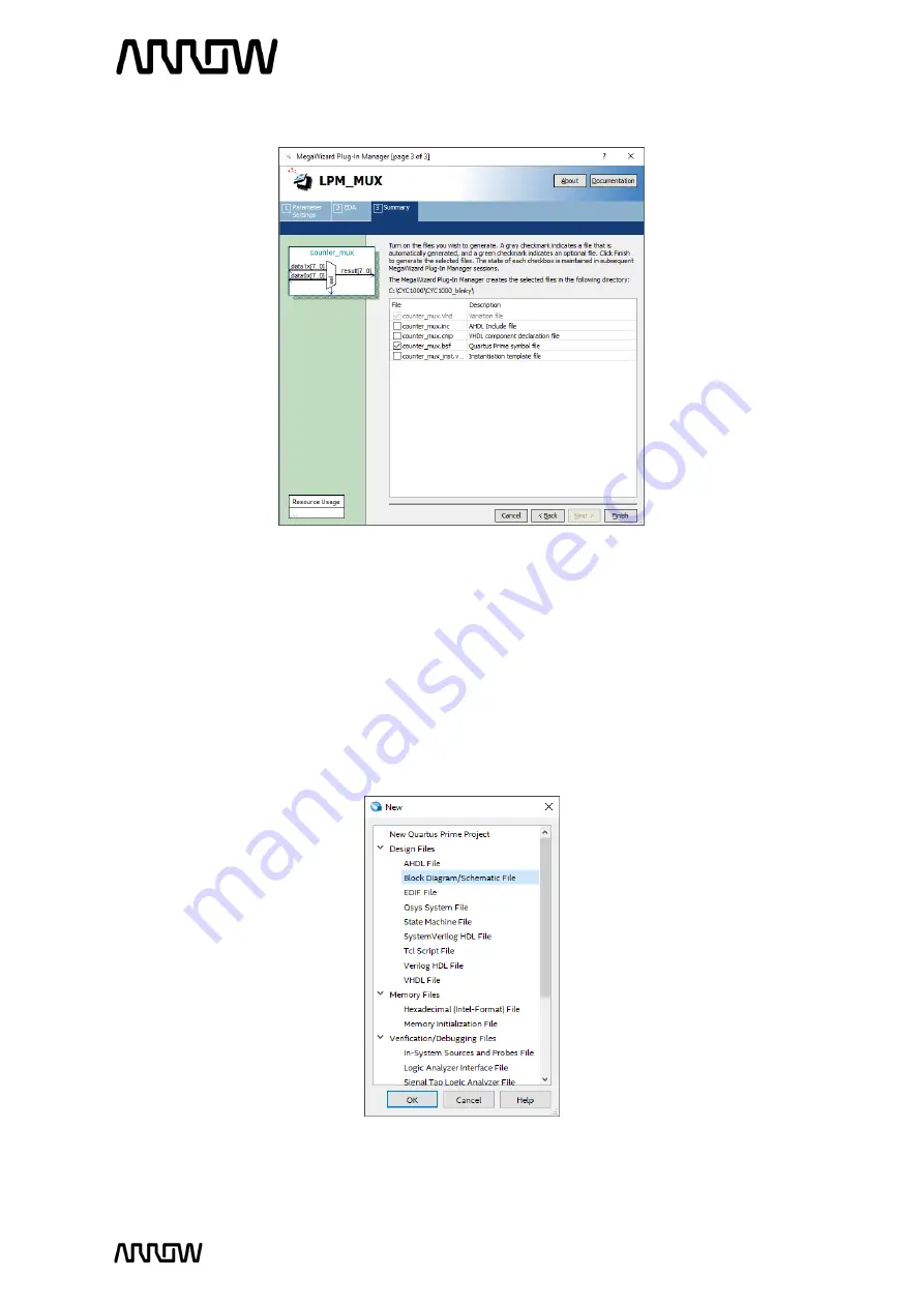
Select counter_mux.bsf checkbox to generate a symbol for our schematic design. 


5.2.7.8


Click 

Finish

”.


5.2.8


Adding the Components to the Schematic 


The next step would be to connect all three components together. 

5.2.8.1


To do so, select File menu, then select New and select Block Diagram/Schematic File. 


5.2.8.2


Click 

OK

”.


A new schematic will be created, where the components can be added. 

Содержание CYC1000

Страница 1: ...CYC1000 User Guide Please read the legal disclaimer at the end of this document Revision 1 0 ...

Страница 2: ... 11 3 3 2 Push Buttons 12 3 3 3 Accelerometer 12 3 3 4 SDRAM Memory 13 3 3 5 Serial Configuration Flash Memory 14 3 3 6 Arduino MKR Connectors 15 3 3 7 PMOD Connector 16 3 3 8 User I O 17 3 3 9 Communication and Configuration 17 3 3 10 Power Tree 19 Software and Driver Installation 20 4 1 Installing Quartus Prime Software 20 4 2 Installing Arrow USB Programmer2 21 New Project with CYC1000 24 5 1 C...

Страница 3: ...3 5 2 11 Analysis and Synthesis 46 5 2 12 Adding Timing Constraints 46 5 2 13 Pinning Assignments 48 5 2 14 Compiling the Design 51 5 2 15 Reading the Compilation Report 52 Configuring the CYC1000 54 6 1 Configure the FPGA in JTAG mode 54 6 2 Serial configuration flash memory programming 57 6 2 1 Programming File generation 58 6 2 2 Device Programming 60 6 3 Testing the Design 62 Common Issues and...

Страница 4: ...YC1000 Clock Tree 10 Figure 5 LED Connections 11 Figure 6 Button Connections 12 Figure 7 Accelerometer Connections 12 Figure 8 SDRAM Connections 13 Figure 9 Flash Connections 14 Figure 10 Arduino MKR Header Connections 15 Figure 11 PMOD Header Connections 16 Figure 12 User I O Connections 17 Figure 13 UART Connections 17 Figure 14 JTAG Connections 18 Figure 15 Power Tree Connections 19 ...

Страница 5: ...e ideal solution for I O expansion chip to chip interfacing industrial automotive and consumer applications The CYC1000 is equipped with an Arrow USB Programmer2 SDRAM flash memory accelerometer sensor and PMOD ADRUINO MKR connectors making it a fully featured plug and play solution without any additional costs The CYC1000 board contains all the tools needed to use the board in conjunction with a ...

Страница 6: ... January 2020 1 3 Getting Help Here are the addresses where you can get help if you encounter any problems Arrow Electronics In Person Arrow EMEA 49 0 6102 5030 0 Online https arrow com Trenz Electronic GmbH https www trenz electronic de en ...

Страница 7: ...ollowing are available on the CYC1000 board Intel Cyclone 10 LP 10CL025YU256C8G device Arrow USB Programmer2 on board for programming JTAG Mode 64MBit SDRAM 166MHz 16Mbit serial configuration flash memory 12MHz MEMS Oscillator One optional MEMS Oscillator of preferred frequency 8x red user LEDs 2x board indication LEDs 2x user push buttons 3 axis accelerometer 12 pin PMOD header Arduino MKR header...

Страница 8: ...A to implement any system design FPGA Device Available Cyclone 10 LP Devices for the CYC1000 Resources Device 10CL006 10CL010 10CL016 10CL025 Logic Elements LE 6 272 10 320 15 408 24 624 M9K Memory Kb 270 414 504 594 18 x 18 Multiplier 15 23 56 66 PLLs 2 2 4 4 Configuration and Debug On board Arrow USB Programmer2 mini USB type B connector Memory Devices 4MBit to 32MBit external flash memory 64MBi...

Страница 9: ...Arduino MKR Header User JTAG Header User I O Header Buttons andIndicators 2x side buttons 8x red user LEDs 2x board indication LEDs Sensors One 3 axis accelerometer Power Recommended external supply voltage range 5 0 V nominal Recommended I O signal voltage range 0 to 3 3 V ...

Страница 10: ...ration data was loaded to Cyclone 10 LP device without error 3 2 Clock Circuitry All the external clocks of the system can be seen in Figure 4 The default clock CLK12M is at 12MHz and is connected and driving the FPGA s user logic and the Arrow USB Programmer2 There is an optional slot of another clock CLK_X to add another preferred clock source to the FPGA Both clocks are driving the internal PLL...

Страница 11: ...EDs There are eight red user controllable LEDs connected to the FPGA Each LED is driven directly and individually by the Cyclone 10 LP FPGA driving its associated pin to a high logic level for on or low logic level for off Board Reference FPGA Pin No I O Standard LED1 PIN_M6 3 3 V LED2 PIN_T4 3 3 V LED3 PIN_T3 3 3 V LED4 PIN_R3 3 3 V LED5 PIN_T2 3 3 V LED6 PIN_R4 3 3 V LED7 PIN_N5 3 3 V LED8 PIN_N...

Страница 12: ... board comes with a digital accelerometer LIS3DH commonly known as the G Sensor This G Sensor is a small thin ultra low power consumption 3 axis accelerometer with digital I2C SPI serial interface standard output The LIS3DH has user selectable full scales of 2g 4g 8g 16g and it is capable of measuring accelerations with output data rates from 1 Hz to 5 kHz The supplied power to the board coming ei...

Страница 13: ...Reference FPGA Pin No Description I O Standard A0 PIN_A3 SDRAM Address 0 3 3 V A1 PIN_B5 SDRAM Address 1 3 3 V A2 PIN_B4 SDRAM Address 2 3 3 V A3 PIN_B3 SDRAM Address 3 3 3 V A4 PIN_C3 SDRAM Address 4 3 3 V A5 PIN_D3 SDRAM Address 5 3 3 V A6 PIN_E6 SDRAM Address 6 3 3 V A7 PIN_E7 SDRAM Address 7 3 3 V A8 PIN_D6 SDRAM Address 8 3 3 V A9 PIN_D8 SDRAM Address 9 3 3 V A10 PIN_A5 SDRAM Address 10 3 3 V...

Страница 14: ... 14 3 3 V DQ15 PIN_A14 SDRAM Data 15 3 3 V DQM0 PIN_B13 SDRAM Lower Data Mask 3 3 V DQM1 PIN_D12 SDRAM Upper Data Mask 3 3 V 3 3 5 Serial Configuration Flash Memory The CYC1000 board supports up to 32MBit of serial flash memory that can be used for user data and programming non volatile storage The configuration bit stream is downloaded into the serial configuration device which automatically load...

Страница 15: ...A Pin No MKR Header Description I O Standard AREF PIN_P11 J1 1 Input reference voltage or GPIO 3 3 V AIN0 PIN_R12 J1 2 GPIO 0 3 3 V AIN1 PIN_T13 J1 3 GPIO 1 3 3 V AIN2 PIN_R13 J1 4 GPIO 2 3 3 V AIN3 PIN_T14 J1 5 GPIO 3 3 3 V AIN4 PIN_P14 J1 6 GPIO 4 3 3 V AIN5 PIN_R14 J1 7 GPIO 5 3 3 V AIN6 PIN_T15 J1 8 GPIO 6 3 3 V D0 PIN_N16 J1 9 Digital In 0 3 3 V D1 PIN_L15 J1 10 Digital In 1 3 3 V D2 PIN_L16 ...

Страница 16: ...er to the connector N A VIN N A J2 13 User power into to the CYC1000 N A 5V N A J2 14 5V power to the connector N A Can only choose one hence same name pinning 3 3 7 PMOD Connector The CYC1000 board offers connectivity to PMOD compatible connectors 2x6 pin or 1x12 pin making it possible to add a big variety of sensors or ICs to the system Below is the connection schematic and pinning information B...

Страница 17: ...h described below 3 3 9 1 UART Communication UART to USB communication supports USB 2 0 High Speed up to 480 Mb s independently of other protocols used in the chip like JTAG Below is the connection schematic and pinning information Board Reference FPGA Pin No Description I O Standard BDBUS0 PIN_R7 Transmitter output of FT2232H Tx 3 3 V BDBUS1 PIN_T7 Receiver input of FT2232H Rx 3 3 V BDBUS2 PIN_R6...

Страница 18: ...provides non volatile storage for the bit stream The information is retained within EPCQ A even if the CYC1000 is turned off When the board is powered on the configuration data in the EPCQ A is automatically loaded into the Cyclone 10 LP FPGA The FPGA device can be configured through JTAG interface on CYC1000 but the JTAG chain must form a closed loop which allows Quartus Prime programmer to detec...

Страница 19: ...he diagram below the board can be powered either by a micro USB connection or by user input voltage from the Arduino MKR header takes precedence over the USB bus All devices are powered by 3 3V voltage line and the 5V and 3 3V lines are fed back to the Arduino header to power that connection if needed The Cyclone 10 LP FPGA is powered by 2 Enpirion devices while a Microchip LDO provides auxiliary ...

Страница 20: ...tems 4 1 Installing Quartus Prime Software 4 1 1 Go to the Intel Download Center Link 4 1 2 Select Windows as the operating system highlighted in red 4 1 3 Select Release 18 1 or your preferred version highlighted in red 4 1 4 Download the following files from the Individual Files tab highlighted in yellow Quartus Prime Lite Edition Free ModelSim Intel FPGA Edition includes Starter Edition Cyclone...

Страница 21: ...these components are selected 4 1 8 Finish the installation of the Quartus Lite and proceeded to the next section to install Arrow USB Programmer2 to be able to connect to the CYC1000 board 4 2 Installing Arrow USB Programmer2 The CYC1000 board uses version 2 of the Arrow USB Programmer2 programming solution that is an FTDI FT2232H Hi Speed USB controller plus a programmer DLL Since this FTDI USB ...

Страница 22: ...rogrammer2 The setup executable installs the programmer DLL and adds some keys to the registry of the PC 4 2 3 After connecting the CYC1000 board to the PC two unknown devices might appear in the Other devices section of device manager of the PC Windows usually automatically finds the appropriate drivers for these devices After some time the Other devices section should be empty Instead two USB Se...

Страница 23: ...isted in the Ports COM LPT section Note The number of the port will most probably be different from the one shown here In case Windows does not automatically find the appropriate drivers go to http www ftdichip com Drivers D2XX htm to download the setup executable to install the required drivers ...

Страница 24: ...aunch Quartus Prime Lite Edition from the Start Menu 5 1 2 In the Quartus Prime tool create a new project File New Project Wizard The New Project Wizard walks you through the project settings such as the name directories files directories device family and other settings These settings can be changed later if needed 5 1 3 Click Next ...

Страница 25: ...ry 2020 5 1 4 Browse in the project directory and choose a preferred location for the new project Then create new folder named CYC1000_blinky This will be the folder containing all the project files 5 1 5 Enter the project name top 5 1 6 Click Next ...

Страница 26: ...ll be created and thus the default settings of empty project should be selected 5 1 8 Click Next 5 1 9 Add Project Files The Add File window will appear For this tutorial new design files will be created so no files will be added For other designs files could be added here 5 1 10 Click Next 5 1 11 Select the Device Part Number of the CYC1000 Board ...

Страница 27: ...kage pin count and speed grade Quartus Prime will use these settings to compile the design and also provide the programming file that you will use later to program the device 5 1 12 Click Next 5 1 13 EDA Tool Settings In the EDA tool Settings window disable any EDA tools if there are any present EDA tools are third party tools that work with Quartus Prime for design entry simulation verification a...

Страница 28: ...ttings can be changed if required at a later time 5 1 16 Click Finish 5 2 Building a Blinky Project with CYC1000 Overview In this section you will create the components to a design make connections set the pins and compile a project The goal is to go through the design process of a simple blinky project where the toggle speed of the LEDs could be controlled by one of the pushbuttons of the CYC1000...

Страница 29: ... components in the following steps will be built separately and then connected together A user push button on the board controls the mux The mux in turn control which of the counter outputs slow counting or fast counting will be shown on the LEDs There are different ways to create components such as RTL or schematic In this lab schematics will be used There are also different ways for entering sch...

Страница 30: ...dow is open by default when you open Quartus Prime If it s not present you can open it by going to the tab Tool IP Catalog 5 2 4 Create a PLL In the IP Catalog browse for ALTPLL via Basic Functions Clocks PLLs and Resets PLL or type in the search field for PLL 5 2 4 1 In the Search bar of the IP Catalog type pll and select ALTPLL which stands for Altera Phase Locked Loop ...

Страница 31: ...ell Both Verilog and VHDL schematics will be created 5 2 4 3 Click OK 5 2 5 Create and Configure the PLL The next step is to configure the PLL component that we just named 5 2 5 1 Enter the PLL reference clock frequency to match the clock input on the CYC1000 Board Since we have a 12 MHz coming into the FPGA the inclk0 input will be 12MHz The setting should look like this 5 2 5 2 Click Next ...

Страница 32: ... by disabling areset and locked outputs The setting should look like this 5 2 5 4 Click Next 5 2 5 5 Continue to select Next to go through the various options e g Pages 3 to Pages 5 but leaving the default options as they are The page numbers can be seen on the top of the window ...

Страница 33: ... default For simplification there is one input to the PLL 12 MHz and one output of the PLL 20 MHz 5 2 5 7 Click Next until reaching page 12 5 2 5 8 On page 12 there is a list of output files that will be generated Since the design will be done in a schematic you will need to select PLL bsf checkbox The bsf file provides a symbol that can be used in the schematic design we will be creating later ...

Страница 34: ...lect Automatically add Quartus Prime IP Files to all projects 5 2 5 12 Click Yes to allow all of the IP to automatically be added to the project and so that this message will not be seen for other designs 5 2 6 Create and Configure the Counter The next step is to create the counter which will drive the LEDs on the CYC1000 board 5 2 6 1 To create this counter select the IP Catalog and expand the Ba...

Страница 35: ...DL as below 5 2 6 4 Click OK 5 2 6 5 The next step is to increase the size of the counter to a number of bits large enough to divide down the clock so we can see the LEDs toggling 5 2 6 6 Change this number to 32 5 2 6 7 Let the counter to be Up only so the LEDs will show the counters counting up 5 2 6 8 Select Next until reaching Page 5 ...

Страница 36: ... 2 7 Create and Configure the Multiplexer The next step is to create a mux component This mux will be used along with a push button on the CYC1000 board to control the speed of the counter where the counter outputs will be seen on the LEDs 5 2 7 1 To create this mux select IP Catalog and expand Basic Functions Miscellaneous and select LPM_MUX or type mux in the search field 5 2 7 2 Click Add ...

Страница 37: ... of the counter_mux and the file type to be VHDL 5 2 7 4 Click OK 5 2 7 5 Select 2 data inputs and the width of the input and output buses to be 8 bits The reason for 8 bits is that there are 8 LEDs to be toggled showing count values The screen should look like this now 5 2 7 6 Click Next until Page 3 ...

Страница 38: ...ur schematic design 5 2 7 8 Click Finish 5 2 8 Adding the Components to the Schematic The next step would be to connect all three components together 5 2 8 1 To do so select File menu then select New and select Block Diagram Schematic File 5 2 8 2 Click OK A new schematic will be created where the components can be added ...

Страница 39: ...hat were created can now be seen 5 2 8 5 Select PLL 5 2 8 6 Click OK 5 2 8 7 The PLL component can be added now by left clicking on the schematic page 5 2 8 8 Just like in the steps from 5 2 8 3 to 5 2 8 6 do the same for counter_mux and simple_counter to add them to the schematic page The order of adding the components does not matter as the connections between them will happen in the following s...

Страница 40: ...our schematic should look similar to the following To place them similarly simply drag the components to the appropriate locations 5 2 9 Connecting the Components Next step is to make the proper connections between the three components we just added to the schematic 5 2 9 1 Select the Node Tool ...

Страница 41: ...ide www arrow com Page 41 January 2020 5 2 9 2 Connect the c0 of the PLL to the simple_counter as shown below This will mean that a single signal c0 is connected to the simple_counter clock 5 2 9 3 Select the Bus Tool ...

Страница 42: ...counter_mux as show below 5 2 9 5 Right click on the output bus of the simple counter that you just created and select Properties Set the name of the bus to counter 31 0 The view of the Bus Properties should look like this 5 2 9 6 Click OK 5 2 9 7 Do the same for input buses of the mux Name the top bus input data1x 7 0 counter 24 31 Name the bottom bus input data0x 7 0 counter 19 26 ...

Страница 43: ...uary 2020 Schematic should look like this 5 2 10 Add inputs outputs to the schematic 5 2 10 1 Click on the Pin Tool as show below and select Input 5 2 10 2 Add one input pin for inclk0 of the PLL and add other one input pin for sel of counter_mux ...

Страница 44: ...e This is going to be the clock signal coming into the FPGA 5 2 10 4 Rename the pin_name2 to USER_BTN by double clicking its current name This is going to be the user button of the CYC1000 board to select the mux 5 2 10 5 Using the Node Tool connect CLK12M inclk0 of the PLL component USER_BTN sel of the counter_mux component Your schematic should look like this now ...

Страница 45: ...unter_mux component and output pin result 7 0 LED 7 0 The final schematic should look like the following Looking at the schematic even though the buses are not connected together by wires the names of counter tell Quartus Prime to connect the signals together Overall the user button will toggle between displaying higher 8 bits of the counter and 8 lower bits of the counter The signals of the count...

Страница 46: ...tart Analysis and Synthesis or from clicking button on the top toolbar There should be no errors If there are errors they should be fixed before continuing and Analysis and Synthesis run again 5 2 12 Adding Timing Constraints Timing Constraints tell the Quartus what are the timing requirements for this design Timing Constraints are required in every CPLD FPGA design 5 2 12 1 To add the timing cons...

Страница 47: ...port in the sdc format The second line derive_pll_clocks tells the software to look if there are any PLLs and if so automatically derive the clock multiplication division of the outputs of the PLL even if they are used internally within the CPLD FPGA The third line derive_clock_uncertainty tells the software to automatically determine the internal clock uncertainty No clock is ideal and thus there...

Страница 48: ...e the design can be downloaded to the FPGA pin assignments that match the hardware on the board are needed There are different ways to do this such as the Pin Planner Assignment Editor and text files The following steps will show one of these ways the Pin Planner Since there are only 10 pins that need to be assigned the Pin Planner can be used If many pins are needed other ways can be used such as...

Страница 49: ... seen below 5 2 13 2 To make pin assignments select the CLK12M node name on the bottom portion and drag and drop it to pin M2 of the Top View of the FPGA or alternatively set the Location field of the CLK12M to PIN_M2 Note that the Location of the CLK12M is now set to Location PIN_M2 as seen in blue colour in the top view of the FPGA ...

Страница 50: ...6 USER_BTN PIN_N6 5 2 13 4 Now the Pin Planner should look like this after assigning all the pin locations 5 2 13 5 The specific pins are now selected but the I O standards now need to be set as well The button LEDS and clock pins are the same I O standard for CYC1000 since all banks and peripherals are powered by 3 3V The USER_BTN the LEDs and clock pins are 3 3 V LVTTL These I O standards can be...

Страница 51: ...gs are automatically saved 5 2 14 Compiling the Design 5 2 14 1 You can set the default I O Standard which can eliminate some design warning and save you time from setting the standard for some pins manually Open Assignments Device Device and Pin Options Voltage and set Default I O Standard to 3 3 V LVTTL and press OK to all the windows ...

Страница 52: ...ilation or push the button on the toolbar If there are errors they will need to be resolved and re compiled before the design can be programmed to the board When Compiling finishes and there are no errors there will be a message at the bottom of the window that states Full Compilation was successful and a 100 indication along with the compile time in the right bottom corner 5 2 15 Reading the Comp...

Страница 53: ...in Resource Usage Summary as well how many LEs were used for each component in Resource Utilization by Entity In the Fitter more detailed information about the pins and their banks can be seen Timing Analyzer shows various timing information concerning the design as well as if the design has met the timing requirements In this case timing requirements were met but in other cases that requirements ...

Страница 54: ... Connect your CYC1000 board to your PC using an USB cable Since the Arrow USB Blaster should be already installed the Window s Device Manager should display the following entries are highlighted in red port number may differ depending on your PC If the Arrow USB Blaster is not installed please refer to Chapter 4 2 for installing the drivers 6 1 2 Open the Quartus Prime Programmer from Tools Progra...

Страница 55: ... Click Hardware Setup and double click Arrow USB Blaster entry in the Hardware Setup tab The Currently selected hardware should now show Arrow USB Blaster USB0 depending on your PC the USB port number may variant 6 1 5 Click Close 6 1 6 Make sure the hardware setup is Arrow USB Blaster USB0 and the mode is JTAG If the Mode is not set to JTAG click on it and select JTAG from the drop down menu ...

Страница 56: ... steps and continue with the 6 1 12 point 6 1 8 Click Auto Detect on the left side of the Programmer 6 1 9 Select 10CL025Y device and click OK on the Select Device window 6 1 10 Double click none to choose programming file 6 1 11 Navigate to project_directory output_files in your compilation directory Select and open the top sof file ...

Страница 57: ...e Progress bar should reach 100 Successful The design is now programmed to the FPGA Note that turning off and then on the FPGA will result into losing its configuration 6 2 Serial configuration flash memory programming The configuration data to be written to EPCQ A will be part of the JTAG indirect configuration file jic This configuration data is automatically loaded from the serial configuration...

Страница 58: ...us Prime go to File Convert Programming Files 6 2 1 2 Set the programming file type to JTAG Indirect Configuration File jic 6 2 1 3 Select EPCQ16A from the drop down menu for configuration device and make sure that the Active Serial is set to mode The output programming file settings should look like this ...

Страница 59: ...ngs and click on Add Device button 6 2 1 5 On the new window select Cyclone 10 LP as Device family and 10CL025Y as Device name 6 2 1 6 Click OK to add device to Flash Loader 6 2 1 7 Select SOF Data under Input files to convert and click on Add File button 6 2 1 8 Go to project_directory output_files and open top sof ...

Страница 60: ... 9 Make sure that your settings are same as the picture below and if everything is correct click Generate 6 2 1 10 Click OK on the successful file generation notification and close Convert Programming File window 6 2 2 Device Programming 6 2 2 1 Open Programmer ...

Страница 61: ...e the Programmer will automatically update the JTAG chain and put EPCQ A flash memory 6 2 2 4 Make sure the Programmer shows the correct file and correct parts in the JTAG chain and check the Program Configure checkbox 6 2 2 5 Click Start to configure EPCQ A The programming could take a while 6 2 2 6 When the programming is finished the CYC000 should be able to keep its configuration data even aft...

Страница 62: ...e FPGA and automatically loads the configuration from EPCQ A 6 3 Testing the Design Does not matter which way the CYC1000 was configured the results should be the same for both methods with the only difference being if configuration is retained after power off On the board by default the LEDS should now toggle in a slow counting sequence Push and hold the USER_BTN to see that the LEDs will now tog...

Страница 63: ...ixes 1 Issue In some rare cases when using Windows 10 operating system the programmer DLL is not properly loaded unloaded causing the Quartus Programmer to not detect the Arrow USB Programmer2 Solution Restart the Altera JTAG Server using the Services application of Windows ...

Страница 64: ...CYC1000 User Guide www arrow com Page 64 January 2020 Appendix 8 1 Revision History Version Change Log Date of Change V1 0 Initial Version 03 02 2020 ...

Страница 65: ... system and it may not be offered for sale or lease or sold leased or otherwise distributed for commercial purposes OWNERSHIP AND COPYRIGHT Title to the Evaluation Board remains with Arrow and or its licensors This Agreement does not involve any transfer of intellectual property rights IPR for evaluation board You may not remove any copyright or other proprietary rights notices without prior writt...

Страница 66: ...nder this Agreement You shall indemnify Arrow and its Affiliates and Licensors against and pay any resulting costs and damages finally awarded against Arrow and its Affiliates and Licensors or agreed to in any settlement provided that You have sole control of the defense and settlement of the claim or action and Arrow cooperates in the defense and furnishes all related evidence under its control a...

Отзывы: