background image

ETM Interface

9-4

Copyright © ARM Limited 2000. All rights reserved.

ARM DDI 0155A

9.2

Enabling the ETM interface

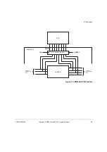
The only input to the ETM interface of the ARM946E-S is an enable signal that 
determines whether the required ARM9E-S inputs and outputs are driven out from the 
ARM946E-S.

The ETM enable is controlled by the top-level pin ETMEN. When this input is HIGH, 
the ETM interface is enabled and the outputs are driven so that an external ETM can 
begin code tracing.

When the ETMEN input is driven LOW, the ETM interface outputs are held at their 
last value before the interface is disabled. At reset, all ETM interface outputs are reset 
LOW.

The ETMEN input is usually driven by the ETM, and driven HIGH when you have 
programmed the ETM using its TAP controller.

Note

If you do not use an ETM in an embedded ARM946E-S design, you must tie the 
ETMEN input LOW to save power.

Содержание ARM946E-S

Страница 1: ...ARM DDI 0155A ARM946E S Technical Reference Manual ...

Страница 2: ... in this document is Final information on a developed product ARM web address http www arm com Change history Date Issue Change 11th August 2000 A First release All other products or services mentioned herein may be trademarks of their respective owners Neither the whole nor any part of the information contained in or the product described in this document may be adapted or reproduced in any mater...

Страница 3: ...urther reading xv Feedback xvi Chapter 1 Introduction 1 1 About the ARM946E S 1 2 1 2 Microprocessor block diagram 1 3 Chapter 2 Programmer s Model 2 1 About the ARM94E S programmer s model 2 2 2 2 About the ARM9E S programmer s model 2 3 2 3 CP15 register map summary 2 4 Chapter 3 Caches 3 1 Cache architecture 3 2 3 2 ICache 3 6 3 3 DCache 3 8 3 4 Cache lockdown 3 12 ...

Страница 4: ... LDC STC 7 4 7 3 MCR MRC 7 8 7 4 Interlocked MCR 7 10 7 5 CDP 7 11 7 6 Privileged instructions 7 12 7 7 Busy waiting and interrupts 7 13 Chapter 8 Debug Support 8 1 About the debug interface 8 2 8 2 Debug systems 8 4 8 3 The JTAG state machine 8 7 8 4 Scan chains 8 12 8 5 Debug access to the caches 8 17 8 6 Debug interface signals 8 19 8 7 ARM9E S core clock domains 8 24 8 8 Determining the core a...

Страница 5: ...C timing parameter definitions A 9 Appendix B Signal Descriptions B 1 Signal properties and requirements B 2 B 2 Clock interface signals B 3 B 3 AHB signals B 4 B 4 Coprocessor interface signals B 6 B 5 Debug signals B 8 B 6 JTAG signals B 10 B 7 Miscellaneous signals B 11 B 8 ETM interface signals B 12 B 9 INTEST wrapper signals B 14 Index ...

Страница 6: ...vi Copyright ARM Limited 2000 All rights reserved ARM DDI 0155A 04 Limited Confidential ...

Страница 7: ...le 2 9 Register 1 control register 2 11 Table 2 10 Programming instruction data cachable bits 2 15 Table 2 11 Programming data bufferable bits 2 16 Table 2 12 Programming instruction and data access permission bits extended 2 17 Table 2 13 Access permission encoding extended 2 17 Table 2 14 Instruction and data access permission bits standard 2 18 Table 2 15 Access permission encoding standard 2 1...

Страница 8: ...le 4 2 Region size encoding 4 4 Table 6 1 Supported burst types 6 4 Table 6 2 Data write modes 6 12 Table 7 1 Handshake encoding 7 7 Table 8 1 Public instructions 8 9 Table 8 2 ARM946E S scan chain allocations 8 12 Table 8 3 Scan chain 1 bits 8 13 Table 8 4 Scan chain 15 addressing mode bit order 8 14 Table 8 5 Mapping of scan chain 15 address field to CP15 registers 8 14 Table 8 6 Coprocessor 14 ...

Страница 9: ...e 8K cache 3 3 Figure 3 2 Access address for a 4KB cache 3 5 Figure 3 3 Register 7 Rd format 3 10 Figure 4 1 ARM946E S protection unit 4 2 Figure 4 2 Overlapping memory regions 4 6 Figure 5 1 SRAM read cycle 5 2 Figure 6 1 Linefetch transfer 6 4 Figure 6 2 Back to back linefetches 6 5 Figure 6 3 Nonsequential uncached accesses 6 6 Figure 6 4 Data burst followed by instruction fetch 6 6 Figure 6 5 ...

Страница 10: ...igure 8 8 Watchpoint entry with data processing instruction 8 21 Figure 8 9 Watchpoint entry with branch 8 22 Figure 8 10 The ARM9E S TAP controller and EmbeddedICE RT 8 26 Figure 8 11 Debug comms channel status register 8 30 Figure 8 12 Coprocessor 14 debug status register format 8 31 Figure 9 1 ARM946E S ETM interface 9 3 Figure A 1 Clock reset and AHB enable timing A 2 Figure A 2 AHB bus reques...

Страница 11: ... Limited 2000 All rights reserved xi Preface This preface introduces the ARM946E S and its reference documentation It contains the following sections About this document on page xii Further reading on page xv Feedback on page xvi ...

Страница 12: ...M946E S Chapter 2 Programmer s Model This chapter describes the programmer s model of the ARM946E S and includes a summary of the ARM946E S coprocessor registers Chapter 3 Caches This chapter describes the ARM946E S cache implementation Chapter 4 Protection Unit This chapter describes the ARM946E S protection unit Chapter 5 Tightly coupled SRAM This chapter describes the requirements and operation...

Страница 13: ... the ARM946E S Typographical conventions The following typographical conventions are used in this document bold Highlights ARM processor signal names within text and interface elements such as menu names Can also be used for emphasis in descriptive lists where appropriate italic Highlights special terminology cross references and citations typewriter Denotes text that can be entered at the keyboar...

Страница 14: ...occur Therefore no additional meaning should be attached unless specifically stated Key to timing diagram conventions Shaded bus and signal areas are undefined so the bus or signal can assume any value within the shaded area at that time The actual level is unimportant and does not affect normal operation Clock Bus stable HIGH to LOW Transient Bus to high impedance Bus change HIGH LOW to HIGH High...

Страница 15: ...n ARM products or if you have questions not answered by this document please contact info arm com or visit our web site at http www arm com ARM publications ARM Architecture Reference Manual ARM DDI 0100 ARM9E S Technical Reference Manual ARM DDI 0165 AMBA Specification Rev 2 0 ARM IHI 0011 Other publications IEEE Std 1149 1 1990 Standard Test Access Port and Boundary Scan Architecture ...

Страница 16: ... about this product please contact your supplier giving the product name a concise explanation of your comments Feedback on the document If you have any comments about this document please send email to errata arm com giving the document title the document number the page number s to which your comments refer a concise explanation of your comments General suggestions for additions and improvements...

Страница 17: ...ht ARM Limited 2000 All rights reserved 1 1 Chapter 1 Introduction This chapter introduces the ARM946E S processor It contains the following sections About the ARM946E S on page 1 2 Microprocessor block diagram on page 1 3 ...

Страница 18: ... CPU interfaces The size of both the instruction and data SRAM are implementor configurable Instruction and data caches The design can be easily modified to allow any combination of caches from 4 Kbytes to 1 Mbyte A protection unit that allows the memory to be segmented and protected in a simple manner ideal for embedded control applications An AMBA AHB bus interface ARM946E S interfaces to the re...

Страница 19: ...igure 1 1 Figure 1 1 ARM946E S block diagram ARM9E S Instruction SRAM Data SRAM System control coprocessor CP15 External coprocessor interface AHB Bus interface unit and write buffer ETM interface IA DA WDATA RDATA INSTR Addr Din Addr Din Data cache Instruction cache Memory protection unit System controller Data cache control Instruction cache control ...

Страница 20: ...te Buffer Instruction SRAM Chapter 5 Tightly coupled SRAM Data SRAM Chapter 5 Tightly coupled SRAM System control coprocessor CP15 Chapter 2 Programmer s Model External coprocessor interface Chapter 7 Coprocessor Interface ETM interface Chapter 9 ETM Interface System controller Chapter 2 Programmer s Model Memory protection unit Chapter 4 Protection Unit Instruction cache Chapter 3 Caches Data cac...

Страница 21: ... Chapter 2 Programmer s Model This chapter describes the programmer s model for the ARM946E S It contains the following sections About the ARM94E S programmer s model on page 2 2 About the ARM9E S programmer s model on page 2 3 CP15 register map summary on page 2 4 ...

Страница 22: ... the ARM946E S CP14 within the ARM9E S core allows software access to the debug communications channel CP15 allows configuration of the caches tightly coupled SRAM protection unit write buffer and other ARM946E S system options such as big or little endian operation The registers defined in CP14 are accessible with MCR and MRC instructions and are described in The debug communications channel on p...

Страница 23: ...s from the base updated Data Abort model implemented by ARM7TDMI The difference in the Data Abort model affects only a very small section of operating system code the Data Abort handler It does not affect user code With the base restored Data Abort model when a Data Abort exception occurs during the execution of a memory access instruction the base register is always restored by the processor hard...

Страница 24: ... Unpredictable 0 Cache type a Unpredictable 0 Tightly coupled memory size a Unpredictable 1 Control Control 2 Cache configuration b Cache configuration b 3 Write buffer control Write buffer control 4 Unpredictable Unpredictable 5 Access permission b Access permission b 6 Protection region base and size a Protection region base and size a 7 Unpredictable Cache operations 8 Unpredictable Unpredictab...

Страница 25: ... location provides access to more than one register The register ac cessed depends on the value of the opcode_2 or CRm field See the register description for details b Separate registers for instruction and data See the register description for details Table 2 1 CP15 register map continued Register Read Write Table 2 2 CP15 abbreviations Term Abbreviation Description Unpredictable UNP For reads th...

Страница 26: ... specifies the coprocessor register to access The CRm field and opcode_2 field specify a particular action when addressing registers Attempting to read from a nonreadable register or writing to a nonwritable register causes unpredictable results The opcode_1 opcode_2 and CRm fields should be zero except when the values specified are used to select the desired operations in all instructions that ac...

Страница 27: ...pe register is accessed by reading CP15 register 0 with the opcode_2 field set to 1 For example MRC p15 0 Rd c0 c0 1 returns cache details The format of the register is shown in Table 2 4 Table 2 3 Register 0 ID code Register bits Function Value 31 24 Implementor 0x41 23 20 Reserved variant 0x00 19 16 Architecture version ARM5TExP 0x04 15 4 Part number 0x946 3 0 Version implementation specific Rev...

Страница 28: ...n cache size Table 2 5 lists the meaning of values used for cache size encoding 11 10 Reserved 00 9 6 ICache size Implementation specific 5 3 ICache associativity Implementation specific 2 ICache base size Implementation specific 1 0 ICache words per line 10 defines 8 words per line Table 2 5 Cache size encoding Bits 21 18 and bits 9 6 Cache size b0000 0KB b0011 4KB b0100 8KB b0101 16KB b0110 32KB...

Страница 29: ...o avoid having to resynthesize the design for different cache sizes Bit 14 gives the data cache base size Bit 2 gives the instruction cache base size The base size bits are implementation specific If the implementation has an instruction or data cache the base size bit for that cache is set to 0 indicating that the cache type parameters are valid If either cache is not included for a specific impl...

Страница 30: ...ize Bits 9 6 define the instruction RAM size Table 2 8 shows the memory size field definitions for instruction and data RAM memory sizes Table 2 7 Tightly coupled memory size register Register bit Meaning Value 31 22 Reserved b0000000000 21 18 Data RAM size Implementation specific 17 15 Reserved b000 14 Data RAM absent Implementation specific 13 10 Reserved b0000 9 6 Instruction RAM size Implement...

Страница 31: ...ed or written using read modify write The reserved bits have an unpredictable value when read To read and write this register MRC p15 0 rd c1 c0 0 read control register MCR p15 0 rd c1 c0 0 write control register Table 2 9 lists the functions controlled by register 1 b1001 256KB b1010 512KB b1011 1MB Table 2 8 Memory size field continued Bits 21 8 and bits 9 6 Tightly coupled RAM size Table 2 9 Re...

Страница 32: ...htly coupled instruction RAM This allows you to copy boot code from memory located at address 0x0 into the instruction RAM which when enabled also exists at address 0x0 The operation of the load mode is described in I SRAM load mode on page 5 4 At reset this bit is cleared Bit 18 Instruction RAM enable This bit controls operation of the tightly coupled instruction RAM When the instruction RAM is e...

Страница 33: ...enable This bit controls operation of the tightly coupled data RAM When the data RAM is enabled it takes precedence over the data cache and AHB for data accesses At reset this bit is cleared Bit 15 Configure disable loading TBIT This bit controls the behavior of load PC instructions When LOW the ARMv5TExP specific behavior is enabled and bit 0 of the loaded data is used to control the entry into T...

Страница 34: ...struction cache both the protection unit enable bit bit 0 and the ICache enable bit must be HIGH This can be done with a single write to register 1 At reset this bit is cleared Bit 7 Endian Selects the endian configuration of the ARM946E S When this bit is HIGH big endian configuration is selected When LOW little endian configuration is selected At reset this bit is cleared Bit 2 DCache enable Thi...

Страница 35: ...ters MRC p15 0 rd c2 c0 0 read data cachable bits MRC p15 0 rd c2 c0 1 read instruction cachable bits MCR p15 0 rd c2 c0 0 write data cachable bits MCR p15 0 rd c2 c0 1 write instruction cachable bits The format for the cachable bits in data and instruction areas is the same and is given in Table 2 10 2 3 7 Register 3 Write buffer control register This register contains the write buffer control bu...

Страница 36: ...instruction or data access permissions are accessed To read and write the extended registers MRC p15 0 rd c5 c0 2 read data access permission bits MRC p15 0 rd c5 c0 3 read instruction access permission bits MCR p15 0 rd c5 c0 2 write data access permission bits MCR p15 0 rd c5 c0 3 write instruction access permission bits The format for the access permission bits in instruction and data areas is ...

Страница 37: ... bits for area 7 27 24 Ap6 3 0 bits for area 6 23 20 Ap5 3 0 bits for area 5 19 16 Ap4 3 0 bits for area 4 15 12 Ap3 3 0 bits for area 3 11 8 Ap2 3 0 bits for area 2 7 4 Ap1 3 0 bits for area 1 3 0 Ap0 3 0 bits for area 0 Table 2 13 Access permission encoding extended I DApn 3 0 Access permission Privileged User 0000 No access No access 0001 Read write access No access 0010 Read write access Read ...

Страница 38: ...struction access permission bits MCR p15 0 rd c5 c0 0 write data access permission bits MCR p15 0 rd c5 c0 1 write instruction access permission bits The data format for these registers is shown in Table 2 14 Table 2 14 Instruction and data access permission bits standard Register bit Function 15 14 Ap7 1 0 bits for area 7 13 12 Ap6 1 0 bits for area 6 11 10 Ap5 1 0 bits for area 5 9 8 Ap4 1 0 bit...

Страница 39: ...age 2 17 and then reprogrammed using the standard access permissions see Table 2 15 on page 2 19 the access permissions applied are as if Apn 3 2 are programmed to 00 in Table 2 13 on page 2 17 2 3 9 Register 6 Protection region base size registers These registers define the protection region base address size registers You can define eight programmable regions using these registers The values are...

Страница 40: ...ictable if this is not done Table 2 16 Accessing protection region base size registers ARM instruction Protection region base size register MCR MRC p15 0 rd c6 c7 0 Memory region 7 MCR MRC p15 0 rd c6 c6 0 Memory region 6 MCR MRC p15 0 rd c6 c5 0 Memory region 5 MCR MRC p15 0 rd c6 c4 0 Memory region 4 MCR MRC p15 0 rd c6 c3 0 Memory region 3 MCR MRC p15 0 rd c6 c2 0 Memory region 2 MCR MRC p15 0 ...

Страница 41: ... Table 2 18 Table 2 18 Area size encoding Bit encoding Area size 00000 to 01010 Reserved UNP 01011 4KB 01100 8KB 01101 16KB 01110 32KB 01111 64KB 10000 128KB 10001 256KB 10010 512KB 10011 1MB 10100 2MB 10101 4MB 10110 8MB 10111 16MB 11000 32MB 11001 64MB 11010 128MB 11011 256MB 11100 512MB 11101 1GB 11110 2GB 11111 4GB ...

Страница 42: ...o 1 are unpredictable 2 3 10 Register 7 Cache operations register A write to this register can be used to perform the following operations flush ICache and DCache prefetch an ICache line wait for interrupt drain the write buffer clean and flush the DCache The ARM946E S uses a subset of the ARM architecture v4 functions defined in the ARM Architecture Reference Manual The available operations are s...

Страница 43: ...S MCR p15 0 rd c7 c14 1 Clean and flush DCache entry Address MCR p15 0 rd c7 c10 2 Clean DCache entry Index segment MCR p15 0 rd c7 c14 2 Clean and flush DCache entry Index segment a The value transferred in Rd should be zero Table 2 19 Cache operations continued ARM instruction Function Data 31 30 29 N 1 N 5 4 0 Should be zero Index SBZ Segment Table 2 20 Index fields for supported cache sizes Ca...

Страница 44: ...s is ensured if a drain write buffer operation separates the store to the peripheral and the enable interrupt functions The drain write buffer operation is invoked by a write to register 7 using the following ARM instruction MCR cp15 0 rd c7 c10 4 drain write buffer This stalls the processor core until any outstanding accesses in the write buffer are completed that is until all data is written to ...

Страница 45: ... S core is guaranteed to take the interrupt before executing the instruction after the wait for interrupt If debug request is used to wake up the system the processor enters debug state before executing any more instructions The write buffer continues to drain until empty while the wait for interrupt operation is executing 2 3 11 Register 9 Cache lockdown registers These registers allow you to loc...

Страница 46: ... is useful for debugging multitasking systems There is a memory region register for each of the tightly coupled memories MRC p15 0 rd c9 c1 0 read data tightly coupled memory MCR p15 0 rd c9 c1 0 write data tightly coupled memory MRC p15 0 rd c9 c1 1 read instruction tightly coupled memory MCR p15 0 rd c9 c1 1 write instruction tightly coupled memory Each tightly coupled memory region register has...

Страница 47: ... in Table 2 23 Table 2 23 Tightly coupled memory area size encoding Bit encoding Tightly coupled memory area size b00011 4KB b00100 8KB b00101 16KB b00110 32KB b00111 64KB b01000 128KB b01001 256KB b01010 512KB b01011 1MB b01100 2MB b01101 4MB b01110 8MB b01111 16MB b10000 32MB b10001 64MB b10010 128MB b10011 256MB b10100 512MB b10101 1GB b10110 2GB b10111 4GB ...

Страница 48: ...on page 2 9 You must program the data tightly coupled memory region registers before you set the data RAM enable bit bit 16 in register 1 see Register 1 Control register on page 2 11 If this is not done the data tightly coupled memory resides at the same location resulting in unpredictable behavior Note If the data tightly coupled memory is located at the same address as the instruction tightly co...

Страница 49: ...Write TAG BIST control register MRC p15 0 rd c15 c0 1 MCR p15 0 rd c15 c0 1 RAM BIST control register MRC p15 1 rd c15 c0 1 MCR p15 1 rd c15 c0 1 Cache RAM BIST control register MRC p15 2 rd c15 c0 1 MCR p15 2 rd c15 c0 1 Table 2 25 Register 15 implementation specific BIST instructions Register Read Write Instruction TAG BIST address register MRC p15 0 rd c15 c0 2 MCR p15 0 rd c15 c0 2 Instruction...

Страница 50: ...f the test state access register are shown in Table 2 26 Data RAM BIST address register MRC p15 1 rd c15 c0 6 MCR p15 1 rd c15 c0 6 Data RAM BIST general register MRC p15 1 rd c15 c0 7 MCR p15 1 rd c15 c0 7 Instruction cache RAM BIST address register MRC p15 2 Rd c15 c0 2 MCR p15 2 Rd c15 c0 2 Instruction cache RAM BIST general register MRC p15 2 Rd c15 c0 3 MCR p15 2 Rd c15 c0 3 Data cache RAM BI...

Страница 51: ...2 11 prevent the respective cache from streaming data to the ARM9E S while the linefill is performed to the cache The linefill still occurs but the prefetched instruction or load data is returned to the core at the end of a linefill 2 3 16 Register 15 Cache debug index register Register 15 gives you access to the test features included within the ARM946E S Additional instructions and operations ar...

Страница 52: ... shows how the index address field size changes for the cache sizes supported by the ARM946E S Note For TAG operations the word address field in the cache debug register is ignored The data format for the TAG read write operations is shown in Figure 2 6 Figure 2 6 Data format TAG read write operations Data TAG read Data MRC p15 3 rd c15 c2 0 Instruction cache write Data MCR p15 3 rd c15 c3 0 Instr...

Страница 53: ...e index and TAG address field sizes change for the cache sizes supported by the ARM946E S Table 2 28 Index fields for supported cache sizes Cache size TAG Index 4KB Addr 31 10 Addr 9 5 8KB Addr 31 11 Addr 10 5 16KB Addr 31 12 Addr 11 5 32KB Addr 31 13 Addr 12 5 64KB Addr 31 14 Addr 13 5 128KB Addr 31 15 Addr 14 5 256KB Addr 31 16 Addr 15 5 512KB Addr 31 17 Addr 16 5 1MB Addr 31 18 Addr 17 5 ...

Страница 54: ...Programmer s Model 2 34 Copyright ARM Limited 2000 All rights reserved ARM DDI 0155A ...

Страница 55: ...ory access time the ARM946E S uses a cache controller an Instruction Cache ICache and a Data Cache DCache This chapter describes the features and behavior of each of these blocks It contains the following sections Cache architecture on page 3 2 ICache on page 3 6 DCache on page 3 8 Cache lockdown on page 3 12 ...

Страница 56: ...tailor the size of these to suit individual applications A range of different cache sizes is supported 0KB 4KB 8KB 16KB 32KB 64KB 128KB 256KB 512KB 1MB You can select the ICache and DCache sizes independently The ICache and DCache are formed from synchronous SRAM and have similar architectures An example 8K cache is shown in Figure 3 1 on page 3 3 ...

Страница 57: ...ted 2000 All rights reserved 3 3 Figure 3 1 Example 8K cache RDATA WDATA Address TAG Set 0 W ord 0 RAM Seg 0 Seg 1 Seg 2 Seg 3 ROW 0 1 2 63 32 32 W ord 1 W ord 2 W ord 3 W ord 4 W ord 5 W ord 6 W ord 7 Addr 31 0 Addr 4 2 Addr 31 11 Addr 10 5 ...

Страница 58: ...s This is an allocate on read miss replacement policy Selection of the segment is performed by a segment counter that can be clocked in a pseudo random manner or in a predictable manner based on the replacement algorithm selected Critical or frequently accessed instructions or data can be locked into the cache by restricting the range of the replacement counter You cannot replace locked lines They...

Страница 59: ...can return a hit during a cache lookup On reset all the valid bits are cleared Dirty bits These are associated with write operations in the DCache and are used to indicate that a cache line contains data that differs from data stored at the address in external memory Data can only be marked as dirty if it resides in a write back protection region 256KB Addr 15 5 Addr 31 16 512KB Addr 16 5 Addr 31 ...

Страница 60: ...must program at least one protection region before you enable the protection unit You can lock critical or frequently accessed instructions into the ICache 3 2 2 ICache operation When enabled the ICache operation is additionally controlled by the Cachable instruction Ci bit stored in the protection unit This selectively enables or disables caching for different memory regions The Ci bit affects IC...

Страница 61: ...ta is from external memory The ARM9E S processor only performs reads from the ICache except during debug operations Flushing the entire cache As shown in Table 2 19 on page 2 22 you can flush the entire ICache using an MCR instruction In this case the contents of the ARM register transferred to CP15 must be zero You can use the following code segment to do this MOV r0 0 Clear r0 MCR p15 r0 c7 c5 0...

Страница 62: ... linefetch causes a cache line to be evicted from the DCache the dirty bit for each half of the victim line is read and if the half line contains valid and dirty data it is written back to the write buffer before the linefill replaces it The Cachable data Cd and Bufferable data Bd bits control the behavior of the DCache For this reason the protection unit must be enabled when the DCache is enabled...

Страница 63: ... hit in the DCache update both the cache and external memory 3 3 3 DCache operation When the DCache is enabled it is searched when the processor performs a load or store If the cache hits on a load data is returned to the cache if the Cd bit is 1 If the cache read misses the Cd bit is examined The meaning of the values of the Cd bit are shown in Table 3 2 Stores that hit in the cache update the ca...

Страница 64: ...u can invalidate the whole DCache flush DCache in one operation without writing back dirty data You can invalidate individual lines without writing back any dirty data flush DCache single entry You can perform cleaning on a line by line basis The data is only written back through the write buffer when a dirty line is encountered and the cleaned line remains in the cache clean DCache single entry Y...

Страница 65: ...4Kbyte DCache MOV r1 0 Initialize segment counter outer_loop MOV r0 0 Initialize line counter inner_loop ORR r2 r1 r0 Generate segment and line address MCR p15 0 r2 c7 c14 2 Clean and flush the line ADD r0 r0 0x20 Increment to next line CMP r0 0x400 Complete all entries in one segment BNE inner_loop If not branch back to inner_loop ADD r1 r1 0x40000000 Increment segment counter CMP r1 0x0 Complete...

Страница 66: ...or data to be locked down is not already in the cache if the caches have been used after the last reset the software must ensure that the cache in question is cleaned if appropriate and then flushed You can carry out lockdown in the DCache using CP15 register 9 ICache lockdown uses both CP15 registers 7 and 9 As described in Cache architecture on page 3 2 the ARM946E S ICache and DCache each compr...

Страница 67: ... is more data to lockdown at the final step the DL bit must be left HIGH and the process repeated The DL bit must only be set LOW when all the lockdown data has been loaded The Dindex bits must be set to the next available segment Note The write to CP15 register 9 must not be executed until the linefill has completed This is achieved by aligning the LDR to the last address of the line ICache lockd...

Страница 68: ...you can use to lock down code in the ICache is Subroutine lock_i_cache r1 contains the start address r2 contains the end address Assumes that r2 r1 fits within one cache set The subroutine performs a lockdown of instructions in the instruction cache It first reads the current lock_down index and then locks down the number of sets required Note This subroutine must be located in a noncachable regio...

Страница 69: ...0 Increment address by a cache line length CMP r2 r1 Reached our end address yet BLT lock_loop If not repeat loop ADD r3 r3 0x1 Increment ICache index BIC r0 r3 0x8000000 Clear lockdown bit and Write index into r0 MCR p15 0 r3 c9 c0 1 Write lockdown register MOV pc lr Return from subroutine error MVN r0 0 Move 0xFFFFFFFF into r0 MOV pc lr Return from subroutine ...

Страница 70: ...Caches 3 16 Copyright ARM Limited 2000 All rights reserved ARM DDI 0155A ...

Страница 71: ...000 All rights reserved 4 1 Chapter 4 Protection Unit This chapter describes the ARM946E S protection unit It contains the following sections About the protection unit on page 4 2 Memory regions on page 4 3 Overlapping regions on page 4 6 ...

Страница 72: ... is programmed using CP15 registers 1 2 3 5 and 6 see CP15 register map summary on page 2 4 4 1 1 Enabling the protection unit Before the protection unit is enabled you must program at least one valid protection region If you do not do this the ARM946E S can enter a state that is recoverable only by reset Setting bit 0 of the CP15 register 1 the control register enables the protection unit When th...

Страница 73: ...To ensure correct operation you must define an area of memory from where code is to be executed that allows both data and instruction accesses The base address and size properties are programmed using CP15 register 6 The format for this is shown in Table 4 1 4 2 1 Region base address The base address defines the start of the memory region You must align this to a region sized boundary For example ...

Страница 74: ...able 4 2 Note Any value less than b01011 programmed in CP15 register 6 bits 5 1 results in unpredictable behavior Table 4 2 Region size encoding Bit encoding Area size 00000 to 01010 Reserved 01011 4KB 01100 8KB 01101 16KB 01110 32KB 01111 64KB 10000 128KB 10001 256KB 10010 512KB 10011 1MB 10100 2MB 10101 4MB 10110 8MB 10111 16MB 11000 32MB 11001 64MB 11010 128MB 11011 256MB 11100 512MB 11101 1GB ...

Страница 75: ...on by programming CP15 registers 2 3 and 5 see Chapter 2 Programmer s Model If an access fails its protection check for example if a User mode application attempts to access a Privileged mode access only region a memory abort occurs The processor enters the abort exception mode branching to the Data Abort or Prefetch Abort vector accordingly The cachable and bufferable bits in CP15 registers 2 and...

Страница 76: ...n the processor performs a data load from address 0x3010 while in User mode the address falls into both region 1 and region 2 as shown by the shaded area in Figure 4 2 Because there is a clash the attributes associated with region 2 are applied Because you are only allowed to perform reads from this region a Data Abort occurs Figure 4 2 Overlapping memory regions 4 3 1 Background regions Overlappi...

Страница 77: ...ide any of the defined regions the ARM946E S protection unit is hard wired to abort the access You can override this behavior by programming region 0 to be a 4GB background region In this way if the address does not fall into any of the other seven regions the access is controlled by the attributes you have specified for region 0 ...

Страница 78: ...Protection Unit 4 8 Copyright ARM Limited 2000 All rights reserved ARM DDI 0155A ...

Страница 79: ...M This chapter describes the tightly coupled SRAM in the ARM946E S It contains the following sections ARM946E S SRAM requirements on page 5 2 Using CP15 control register on page 5 3 For details of the ARM9E S interface signals referenced in this chapter see the ARM9E S Technical Reference Manual ...

Страница 80: ...l tables during execution the data interface of the ARM9E S core must be able to access the I SRAM This means that the ARM946E S must multiplex the instruction and data addresses before entering the I SRAM It also means that the instruction data is routed to both the instruction and data interfaces of the core See Figure 1 1 on page 1 3 for details of this data and address multiplexing Figure 5 1 ...

Страница 81: ...SRAM greatly increases the performance of the ARM946E S because the majority of accesses to it can be performed with no stall cycles Accessing the AHB however can cause several stall cycles for each access Note You must take care to ensure that the I SRAM is appropriately initialized before it is enabled and used to supply instructions to the ARM9E S core If the core tries to execute instructions ...

Страница 82: ...load mode is as follows 1 Enable the I SRAM and instruction load mode 2 Load ARM registers from main memory data cache or data RAM 3 Store ARM registers into I SRAM 4 Increment address pointers and repeat load store steps until the code image has been copied A suggested assembler code sequence for this procedure is MOV R0 0 Initialize pointer LDR R1 ImageTop Define end of code image MRC p15 0 R2 c...

Страница 83: ...AM load mode You must initialize the D SRAM with the required data image before use You can initialize the D SRAM by writing to the memory from the AM9E S core data interface The D SRAM load mode allows this to be done in an efficient manner Using the load mode allows you to copy from an address in the data cache or external memory into the same address within the D SRAM The D SRAM load mode bit o...

Страница 84: ...A R0 R2 R9 Store 8 regs into instruction SRAM CMP R1 R0 Check if limit reached BGT CopyLoop Repeat if more to do SWP and SWPB operations to the data tightly coupled memory while it is in load mode have unpredictable results The read accesses external memory or the data cache and the write updates the data tightly coupled memory SWP and SWPB operations must not be performed to addresses in the inst...

Страница 85: ...e Buffer This chapter describes the ARM946E S Bus Interface Unit BIU and write buffer It contains the following sections About the BIU and write buffer on page 6 2 AHB bus master interface on page 6 3 Noncached Thumb instruction fetches on page 6 8 AHB clocking on page 6 9 The write buffer on page 6 12 ...

Страница 86: ...is bus architecture The ARM946E S BIU implements a fully compliant AHB bus master interface and incorporates a write buffer to increase system performance The BIU is the link between the ARM9E S core with the caches and tightly coupled SRAM and the external AHB memory The AHB memory must be accessed for cache linefills and for initializing the tightly coupled memories and to access code and data t...

Страница 87: ...ta cycle the address and control for the next transfer are driven out This leads to a fully pipelined address architecture When an access is in its data cycle a slave can extend an access by driving the HREADY signal LOW This stretches the current data cycle and therefore the pipelined address and control for the next transfer is also stretched This provides a system where all AHB masters and slav...

Страница 88: ... to a cachable area misses in the cache the ARM946E S performs a linefetch A linefetch transfer is shown in Figure 6 1 Figure 6 1 Linefetch transfer Table 6 1 Supported burst types Burst type HBURST encoding Use SINGLE 000 Single writes STR STRH STRB Uncached single reads Uncached instruction fetches INCR 001 Store multiple STM Uncached burst reads LDM INCR4 011 Dirty half cache line write back IN...

Страница 89: ...structions core execution is advanced during the linefetch To allow for cache look ups when crossing a cache line boundary the ARM946E S must insert IDLE cycles onto the AHB bus The effect of this is shown in Figure 6 2 It is assumed in Figure 6 2 that HGRANT is asserted throughout and that the HCLK frequency is the same as CLK Figure 6 2 Back to back linefetches 6 2 6 Uncached transfers If a memo...

Страница 90: ...4 shows a data burst followed by an uncached instruction fetch Figure 6 4 Data burst followed by instruction fetch 6 2 8 Bursts crossing 1KB boundary The AHB specification requires that bursts must not continue across a 1KB boundary Linefetches and cache line write backs cannot cross a 1KB boundary because the start address is aligned to either a four or eight word boundary and the burst length is...

Страница 91: ... Uncached data bursts can cross a 1 KB boundary An example of this is shown in Figure 6 5 The burst is restarted by inserting a nonsequential transfer as the boundary is crossed Figure 6 5 Crossing a 1KB boundary CLK HTRANS HADDR NSEQ SEQ SEQ SEQ NSEQ SEQ IDLE 0x3F0 0x3F4 0x3F8 0x3FC 0x400 0x404 0x404 ...

Страница 92: ...fetches Thumb instruction fetches are performed as 32 bit accesses on the AHB interface To minimize bus loading AHB transfers are only performed for nonsequential addresses and for sequential addresses that cross a word boundary The word returned from main memory is latched so that both halfwords are available for the processor core ...

Страница 93: ...ansfer has completed As the AHB system is being clocked by the lower rate HCLK HCLKEN is examined to detect when to drive out the AHB address and control to start an AHB transfer HCLKEN is then required to detect the following rising edges of HCLK so that the BIU knows the access has completed If the slave being accessed at the HCLK rate has a multi cycle response the HREADY input to the ARM946E S...

Страница 94: ...erted to allow an evenly distributed clock to be driven to all the registers in the design The registers that drive out AHB outputs and sample AHB inputs are therefore timed off CLK at the bottom of the inserted clock tree and subject to the clock tree insertion delay To maximize performance when the ARM946E S is embedded in an AHB system the clock generation logic to produce HCLK must be constrai...

Страница 95: ... to match CLK for optimal performance Hierarchical clock tree insertion If you perform clock tree insertion on the ARM946E S before it is embedded you can add buffers on input data to match the clock tree so that the setup and hold is relative to the top level CLK This is guaranteed to be safe at the expense of extra buffers in the data input path The HCLK domain AHB peripherals must still meet th...

Страница 96: ... attribute of the protection region AND the DCache enable AND the protection unit enable Bd bit This is generated from the bufferable attribute for the protection region AND the protection unit enable All accesses are initially noncachable and nonbufferable until you have programmed and enabled the protection unit Therefore you cannot use the write buffer while the protection unit is disabled On r...

Страница 97: ...er Writes cannot be externally aborted DCache linefills cause the write buffer to drain before the linefill starts WB Searches the DCache for reads and writes Reads that miss in the DCache cause a line fill Reads that hit in the DCache do not perform an external access Writes that miss in the DCache are buffered Writes that hit in the DCache update the cache line mark it as dirty and do not send t...

Страница 98: ...Bus Interface Unit and Write Buffer 6 14 Copyright ARM Limited 2000 All rights reserved ARM DDI 0155A ...

Страница 99: ...hapter describes the ARM946E S pipelined coprocessor interface It contains the following sections About the coprocessor interface on page 7 2 LDC STC on page 7 4 MCR MRC on page 7 8 Interlocked MCR on page 7 10 CDP on page 7 11 Privileged instructions on page 7 12 Busy waiting and interrupts on page 7 13 ...

Страница 100: ... stalls the ARM9E S pipeline so the the external coprocessor pipeline can catch up with the processor pipeline So practically consider that the two pipelines are synchronized The ARM9E S core informs the coprocessor when instructions move from Decode into Execute and whether the instruction has to be executed To enable coprocessors to continue executing coprocessor data operations while the ARM9E ...

Страница 101: ...ocessor or store from coprocessor to memory MCR MRC Register transfer between coprocessor and ARM processor core CDP Coprocessor data operation The following sections give examples of how a coprocessor must execute these instruction classes LDC STC on page 7 4 MCR MRC on page 7 8 Interlocked MCR on page 7 10 CDP on page 7 11 Privileged instructions on page 7 12 Busy waiting and interrupts on page ...

Страница 102: ...ansferred The number of words transferred is determined by how the coprocessor drives the CHSDE 1 0 and CHSEX 1 0 buses As with all other instructions the ARM9E S performs the main Decode off the rising edge of the clock during the Decode stage From this the core commits to executing the instruction and so performs an instruction Fetch The coprocessor instruction pipeline keeps in step with ARM9E ...

Страница 103: ...if the instruction in the Execute stage of the coprocessor pipeline is a coprocessor instruction has passed its condition codes If a coprocessor instruction busy waits CPPASS is asserted on every cycle until the coprocessor instruction is executed If an interrupt occurs during busy waiting CPPASS is driven LOW and the coprocessor stops execution of the coprocessor instruction Another output CPLATE...

Страница 104: ...o the instruction it must not change any coprocessor state until it has seen CPPASS HIGH at the same time as the handshake signals indicate the GO or LAST condition GO The GO state indicates that the coprocessor can execute the instruction immediately and that it requires another cycle of execution Both the ARM9E S processor core and the coprocessor must also consider the state of the CPPASS signa...

Страница 105: ...uts must be tied off to indicate ABSENT 7 2 3 Multiple external coprocessors If multiple external coprocessors are to be attached to the ARM946E S interface you can combine the handshaking signals by ANDing bit 1 and ORing bit 0 In the case of two coprocessors that have handshaking signals CHSDE1 CHSEX1 and CHSDE2 CHSEX2 respectively CHSDE 1 CHSDE1 1 AND CHSDE2 1 CHSDE 0 CHSDE1 0 OR CHSDE2 0 CHSEX...

Страница 106: ... instruction on CPINSTR 31 0 is entering the Decode stage of the pipeline This causes the coprocessor to decode the new instruction and drive CHSDE 1 0 as required In the next cycle nCPMREQ is driven LOW to denote that the instruction has now been issued to the Execute stage If LAST Ignored WAIT CLK nCPMREQ CPINSTR 31 0 CHSDE 1 0 CHSEX 1 0 CPDOUT 31 0 MCR CPPASS CPLATECANCEL MCR MRC CPDIN 31 0 MRC...

Страница 107: ...ined It is ignored in all other cases For any successive Execute cycles the CHSEX 1 0 handshake bus is examined When the LAST condition is observed the instruction is committed In the case of an MCR the CPDOUT 31 0 bus is driven with the registered data during the coprocessor Write stage In the case of an MRC CPDIN 31 0 is sampled at the end of the ARM9E S core Memory stage and written to the dest...

Страница 108: ... is the destination from a preceding LDR instruction In this situation the MCR instruction enters the Decode stage of the coprocessor pipeline and then remains there for a number of cycles before entering the Execute stage Figure 7 4 gives an example of an interlocked MCR that also has a busy wait state Figure 7 4 Interlocked MCR MRC timing with busy wait LAST Ignored WAIT CLK nCPMREQ CPINSTR 31 0...

Страница 109: ...h LAST If the instruction requires a busy wait cycle the coprocessor drives CHSDE 1 0 with WAIT and then CHSEX 1 0 with LAST Figure 7 5 shows a CDP cancelled because the previous instruction caused a Data Abort Figure 7 5 Late cancelled CDP The CDP instruction enters the Execute stage of the pipeline and is signaled to execute by CPASS In the following cycle CPLATECANCEL is asserted This causes th...

Страница 110: ...a mode change Figure 7 6 Privileged instructions The first two CHSDE 1 0 responses are ignored by the ARM9E S because it is only the final CHSDE 1 0 response as the instruction moves from Decode into Execute that counts This allows the coprocessor to change its response as nCPTRANS changes Ignored Ignored CLK nCPMREQ CPINSTR 31 0 CHSDE 1 0 CHSEX 1 0 CPPASS CPLATECANCEL CPRT Decode Decode Decode Ex...

Страница 111: ...ion in the busy wait loop For interrupt latency reasons the coprocessor can be interrupted while busy waiting This causes the instruction to be abandoned Abandoning execution is done through CPPASS The coprocessor must monitor the state of CPPASS during every busy wait cycle If it is HIGH the instruction must still be executed If it is LOW the instruction must be abandoned Figure 7 7 shows a busy ...

Страница 112: ...Coprocessor Interface 7 14 Copyright ARM Limited 2000 All rights reserved ARM DDI 0155A ...

Страница 113: ...G state machine on page 8 7 Scan chains on page 8 12 Debug access to the caches on page 8 17 Debug interface signals on page 8 19 ARM9E S core clock domains on page 8 24 Determining the core and system state on page 8 25 The ARM9E S EmbeddedICE RT logic is also discussed in this chapter including Overview of EmbeddedICE RT on page 8 26 Disabling EmbeddedICE RT on page 8 28 The debug communications...

Страница 114: ...alt mode operation and allows you to examine the internal state of the ARM9E S core ARM946E S system and external AHB state while all other system activity continues as normal When debug has been completed the ARM9E S restores the core and system state and resumes program execution The examination of the internal state of the ARM946E S uses a JTAG style interface that allows you to serially insert...

Страница 115: ... macrocell you must use a three stage synchronizer The off chip device for example Multi ICE issues a TCK signal and waits for the RTCK Returned TCK signal to come back Synchronization is maintained because the off chip device does not progress to the next TCK until after RTCK is received Figure 8 1 shows this synchronization Figure 8 1 Clock synchronization D Q D Q D Q D Q D Q TDO RTCK TCK TMS TD...

Страница 116: ... typically has three parts The debug host The protocol converter on page 8 5 ARM946E S debug target on page 8 5 The debug host and the protocol converter are system dependent 8 2 1 The debug host The debug host is a computer that is running a software debugger such as armsd The debug host allows you to issue high level commands such as setting breakpoints or examining the contents of memory Host c...

Страница 117: ...e extensions that ease debugging at the lowest level The debug extensions allow you to stall the core from program execution examine the core internal state examine the state of the memory system resume program execution The following major blocks of the ARM9E S are shown in the ARM9E S block diagram on page 8 6 ARM9E S CPU core With hardware support for debug EmbeddedICE RT logic This is a set of...

Страница 118: ...the ARM946E S by the addition of scan chain 15 This is used for debug access to the CP15 register bank to allow you to configure the system state within the ARM946E S while in debug state for instance to enable or disable the SRAM before performing a debug load or store ARM9E S TAP Controller ARM9E S ARM9E S EmbeddedICE RT logic Scan chain 2 Scan chain 1 ...

Страница 119: ...SM 3 0 bits Figure 8 4 Test access port TAP controller state transitions1 Select DR Scan 0x7 Capture DR 0x6 Shift DR 0x2 Exit1 DR 0x1 Pause DR 0x3 Exit2 DR 0x0 Update DR 0x5 Run Test Idle 0xC Test Logic Reset 0xF tms 0 tms 0 tms 1 tms 0 tms 1 tms 1 Select IR Scan 0x4 Capture IR 0xE Shift IR 0xA Exit1 IR 0x9 Pause IR 0xB Exit2 IR 0x8 Update IR 0xD tms 0 tms 0 tms 1 tms 0 tms 1 tms 1 tms 0 tms 0 tms...

Страница 120: ... from debug state The boundary scan chain cells do not intercept any of the signals passing between the external system and the core 2 The IDCODE instruction is selected If the TAP controller is put into the SHIFT DR state and TCK is pulsed the contents of the ID register are clocked out of TDO 8 3 2 Pull up resistors The IEEE 1149 1 standard effectively requires TDI and TMS to have internal pull ...

Страница 121: ...EST instruction all the scan cells are placed in their test mode of operation In the CAPTURE DR state inputs from the system logic and outputs from the output scan cells to the system are captured by the scan cells In the SHIFT DR state the previously captured test data is shifted out of the scan chain on TDO while new test data is shifted in on the TDI input This data is applied immediately to th...

Страница 122: ...gic to the input scan cells is captured In the SHIFT DR state the previously captured test data is shifted out of the scan chain on the TDO pin while new test data is shifted in on the TDI pin IDCODE 1110 The IDCODE instruction connects the device identification register or ID register between TDI and TDO The ID register is a 32 bit register that allows the manufacturer part number and version of ...

Страница 123: ...cted scan chain are placed in the normal mode of operation In the CAPTURE DR state a snapshot of the signals of the boundary scan is taken on the rising edge of TCK Normal system operation is unaffected In the SHIFT DR state the sampled test data is shifted out of the boundary scan on the TDO pin while new data is shifted in on the TDI pin to preload the boundary scan parallel input latch This dat...

Страница 124: ...an chains are listed in Table 8 2 8 4 1 Scan chain 1 This scan chain is primarily used for debugging and provides access to the core instruction and data buses Scan chain 1 is 67 bits long and is made up of 32 bits for data values 3 control bits 32 bits for instruction data Table 8 2 ARM946E S scan chain allocations Scan chain number Function 0 Reserved 1 Debug 2 EmbeddedICE RT logic programming 3...

Страница 125: ...hpoint condition occurs the WPTANDBKPT bit must be examined by the debugger to determine whether the instruction currently in the Execute stage of the pipeline is breakpointed If it is WPTANDBKPT is HIGH otherwise it is LOW 8 4 2 Scan chain 2 Scan chain 2 allows access to the EmbeddedICE RT logic registers The order of the scan chain from DBGTDI to DBGTDO is read write register address bits 4 0 da...

Страница 126: ...mapping of the CP15 register address field of scan chain 15 to CP15 registers is shown in Table 8 5 Table 8 4 Scan chain 15 addressing mode bit order Bits Contents 38 Read 0 write 1 37 32 CP15 register address 31 0 CP15 data value Table 8 5 Mapping of scan chain 15 address field to CP15 registers Address Register 37 36 33 32 Number Name Type 0 0000 0 C0 ID ID register Read 0 0000 1 C0 C Cache type...

Страница 127: ...down Read write 0 1001 1 C9 I Instruction cache lock down Read write 1 1000 1 C9 Dram Data SRAM size location Read write 1 1001 1 C9 Iram Instruction SRAM size location Read write 0 1101 1 C13 TPID Trace process identifier Read write 0 1111 0 C15 State Test state Read write 0 1111 1 C15 TAG TAG BIST control Read write 1 1111 1 C15 RAM Cache RAM BIST control Read write 1 1101 0 C15 C Ind Cache inde...

Страница 128: ...E DR state is reached For reading return to SHIFT DR through CAPTURE DR to shift out the register value 0 1011 0 C15 DT Data tag read write uses C15 C Ind Read write 0 1011 1 C15 IT Instruction tag read write uses C15 C Ind Read write 1 1110 1 C15 Mem Memory RAM BIST control Read write a For CP15 register 6 CRm corresponds to the region number 0 to 7 Table 8 5 Mapping of scan chain 15 address fiel...

Страница 129: ... set within the cache The format of the data returned is shown in Figure 8 5 Figure 8 5 TAG address format The TAG address is formed from the TAG contents and the TAG index used to interrogate the TAG This ensures that the data format returned is consistent regardless of cache size Step 2 Reading individual entries using the CP15 scan chain can be useful where an entry has been marked as dirty bec...

Страница 130: ...e index register format Note Although 27 bits are specified for the TAG address only those bits required for the TAG implemented are used The cache index register is also used for writing to the instruction cache This is useful for setting software breakpoints within code already in the cache This means that you do not have to flush the cache and reload the entry Note There is no mechanism for det...

Страница 131: ...own in Figure 8 7 Figure 8 7 Breakpoint timing You can build external logic such as additional breakpoint comparators to extend the breakpoint functionality of the EmbeddedICE RT logic The output from the external logic must be applied to the DBGIEBKPT input This signal is ORed with the internally generated Breakpoint signal before being applied to the ARM9E S core control logic The timing of the ...

Страница 132: ...uction is discarded When the interrupt has been serviced the execution flow is returned to the original program This means that the previously breakpointed instruction is fetched again and if the breakpoint is still set the processor enters debug state when it reaches the Execute stage of the pipeline When the processor has entered halt mode debug state it is important that additional interrupts d...

Страница 133: ...to instruction 5 the next instruction in the code sequence that has not yet been executed The instruction following the instruction that generated the watchpoint might modify the Program Counter PC If this happens you cannot determine the instruction that caused the watchpoint However you can always restart the processor A timing diagram showing debug entry after a watchpoint where the next instru...

Страница 134: ...ocessor enters debug state If there is an interrupt pending the ARM9E S allows the exception entry sequence to occur and then enters debug state 8 6 5 Debug request A debug request can take place through the EmbeddedICE RT logic or by asserting the EDBGRQ signal The request is synchronized and passed to the processor Debug request takes priority over any pending interrupt Following synchronization...

Страница 135: ...rating in halt mode 8 6 6 Actions of the ARM9E S in debug state When the ARM9E S is in debug state both memory interfaces indicate internal cycles This ensures that the tightly coupled SRAM within the ARM946E S and the AHB interface are both quiescent allowing the rest of the AHB system to ignore the ARM9E S and function as normal Because the rest of the system continues operation the ARM9E S igno...

Страница 136: ...omains The ARM9E S has a single clock CLK that is qualified by two clock enables SYSCLKEN controls access to the memory system DBGTCKEN controls debug operations During normal operation SYSCLKEN conditions CLK to clock the core When the ARM946E S is in debug state DBGTCKEN conditions CLK to clock the core ...

Страница 137: ...amine the core and system state by forcing the load and store multiples into the instruction pipeline Before you can examine the core and system state the debugger must determine whether the processor entered debug from Thumb state or ARM state by examining bit 4 of the EmbeddedICE RT debug status register When bit 4 is HIGH the core has entered debug from Thumb state ...

Страница 138: ...ustrates the relationship between the core EmbeddedICE RT and the TAP controller showing only the signals that are pertinent to EmbeddedICE RT Figure 8 10 The ARM9E S TAP controller and EmbeddedICE RT The EmbeddedICE RT logic comprises two real time watchpoint units two independent registers the debug control register the debug status register debug comms channel TAP EmbeddedICE RT ARM9E S DBGTCKE...

Страница 139: ... instructions by the core Execution halts when the values programmed into EmbeddedICE RT match the values currently appearing on the address bus data bus and various control signals Note You can mask bits so that their values do not affect the comparison You can configure each watchpoint unit to be either a watchpoint monitoring data accesses or a breakpoint monitoring instruction fetches Watchpoi...

Страница 140: ...8 10 Disabling EmbeddedICE RT You can disable EmbeddedICE RT by setting the DBGEN input LOW Caution Hard wiring the DBGEN input LOW permanently disables debug access When DBGEN is LOW it inhibits DBGDEWPT DBGIEBKPT and EDBGRQ to the core and DBGACK from the ARM946E S is always LOW ...

Страница 141: ...essor and the asynchronous debugger These registers are located in fixed locations in the EmbeddedICE RT logic register map and are accessed from the processor using MCR and MRC instructions to coprocessor 14 In addition to the comms channel registers the processor can access a 1 bit debug status register for use in the real time debug configuration 8 11 1 Debug comms channel registers CP14 contai...

Страница 142: ...w data can be written If the register is not free W 1 the processor must poll until W 0 From the point of view of the debugger when W 1 some new data has been written that can then be scanned out Bit 0 Denotes whether there is new data in the comms data read register If from the point of view of the processor R 1 there is new data that can be read using an MRC instruction From the point of view of...

Страница 143: ... bit wide read write register with the format shown in Figure 8 12 Figure 8 12 Coprocessor 14 debug status register format Bit 0 of the register the DbgAbt bit indicates whether the processor took a Prefetch or Data Abort in the past because of a breakpoint or watchpoint If the ARM9E S core takes a Prefetch Abort as a result of a breakpoint or watchpoint then the bit is set If on a particular inst...

Страница 144: ...rough the JTAG interface When the debugger sees that the W bit is set it can read the comms data write register and scan the data out The action of reading this data register clears the debug comms control register W bit At this point the communications process can begin again Receiving a message from the debugger Transferring a message from the debugger to the processor is similar to sending a me...

Страница 145: ... Privileged mode access DnTRANS InTRANS read write access watchpoints access size breakpoints ITBIT watchpoints DMAS 1 0 The single step hardware is not enabled External breakpoints watchpoints are not supported You can use the vector catching hardware but must not configure it to catch the Prefetch or Data Abort exceptions No support is provided to mix halt mode monitor mode debug functionality W...

Страница 146: ...a in others then you must 1 Disable that watchpoint unit using the control register for that watchpoint unit 2 Change the other registers 3 Re enable the watchpoint unit by rewriting the control register 8 12 1 Further reading debug in depth A more detailed description of the ARM9E S debug features and JTAG interface are provided in the ARM9E S Technical Reference Manual Appendix D Debug in Depth ...

Страница 147: ...2000 All rights reserved 9 1 Chapter 9 ETM Interface This chapter describes the ARM946E S Embedded Trace Macrocell ETM interface It contains the following sections About the ETM interface on page 9 2 Enabling the ETM interface on page 9 4 ...

Страница 148: ...es An extensible specification exists allowing you to specify the exact set of trigger resources required for a particular application Resources include address and data comparators counters and sequencers The ETM compresses the trace information and exports it through the trace port An external Trace Port Analyzer TPA is used to capture the trace information The ETM interface is primarily one way...

Страница 149: ... ARM DDI 0155A Copyright ARM Limited 2000 All rights reserved 9 3 Figure 9 1 ARM946E S ETM interface ETM ARM9E S To from ARM946E S logic To from ARM946E S logic ETM interface registers CLK nRESET ARM946E S ETMEN En ...

Страница 150: ...ETMEN When this input is HIGH the ETM interface is enabled and the outputs are driven so that an external ETM can begin code tracing When the ETMEN input is driven LOW the ETM interface outputs are held at their last value before the interface is disabled At reset all ETM interface outputs are reset LOW The ETMEN input is usually driven by the ETM and driven HIGH when you have programmed the ETM u...

Страница 151: ...Test Support This chapter describes the test methodology used for the ARM946E S synthesized logic and tightly coupled SRAM It contains the following sections About the ARM946E S test methodology on page 10 2 Scan insertion and ATPG on page 10 3 BIST of memory arrays on page 10 5 ...

Страница 152: ...A 10 1 About the ARM946E S test methodology To achieve a high level of fault coverage you can use scan insertion and ATPG techniques on the ARM9E S core and ARM946E S control logic as part of the synthesis flow You can use BIST to provide high fault coverage of the compiled SRAM ...

Страница 153: ...ion is performed early in the synthesis cycle and the design re optimized with the scan elements in place 10 2 1 ARM946E S INTEST wrapper In addition to the auto inserted scan chains ARM946E S includes a dual purpose INTEST scan chain wrapper This facilitates ATPG and provides an additional method for activating BIST of the SRAM ATPG You can use the INTEST scan chain to enable an ATPG tool to acce...

Страница 154: ...s scanned in to read the BIST control register to check the test result The INTEST wrapper allows the full range of BIST tests to be applied as detailed in BIST of memory arrays on page 10 5 The flow for generating the serialized patterns from ARM assembler source is supplied with the ARM946E S implementation scripts ...

Страница 155: ...T test corrupts the contents of the SRAM being tested You can achieve full programmer control over the BIST mechanism through five registers that are mapped to CP15 register 15 address space For details of the MCR MRC instructions used to access these registers see Register 15 RAM and TAG BIST test registers on page 2 29 10 3 1 BIST control register The CP15 register 15 BIST control register contr...

Страница 156: ...unctionality testing of the BIST hardware changing the seed data for a BIST test providing a nonzero starting address for a BIST test peek and poke of the SRAM returning an address location for a failed BIST test This additional functionality is most useful for debugging faulty silicon during production test The exception to this is the start address for a BIST test It is possible that BIST of the...

Страница 157: ... corrupted with an MCR to the relevant BIST address register 2 Write the corrupted data using a MCR to the BIST general register Table 10 1 Instruction BIST address and general registers BIST register IBIST pause Read Write IBIST address register 0 IBIST fail address IBIST start address IBIST address register 1 IBIST fail address IBIST peek poke address IBIST general register 0 IBIST fail data IBI...

Страница 158: ... predetermined points of the BIST algorithm for instance when the algorithm has reached the top or the bottom of the memory array being tested You can poll the BIST control register to detect when a test has paused the running flag is LOW You can then corrupt the data as described in Pause modes on page 10 7 before you restart the BIST test User pause If the pause bit is clear when the test is act...

Страница 159: ...imited 2000 All rights reserved A 1 Appendix A AC Parameters This appendix lists the AC timing parameters for the ARM946E S It contains the following sections Timing diagrams on page A 2 AC timing parameter definitions on page A 9 ...

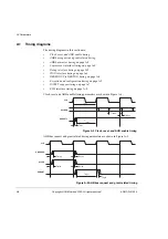
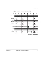
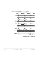
Страница 160: ...iming on page A 6 DBGSDOUT to DBGTDO timing on page A 6 Exception and configuration timing on page A 7 INTEST wrapper timing on page A 7 ETM interface timing on page A 8 Clock reset and AHB enable timing parameters are shown in Figure A 1 Figure A 1 Clock reset and AHB enable timing AHB bus request and grant related timing parameters are shown in Figure A 2 Figure A 2 AHB bus request and grant rel...

Страница 161: ...rs are shown in Figure A 3 Figure A 3 AHB bus master timing CLK HRESP HREADY HTRANS 1 0 ovtr T HADDR 31 0 HWRITE HSIZE 2 0 HBURST 2 0 HPROT 3 0 HWDATA 31 0 NONSEQ A Control Write data A ohtr T ova T oha T ovctl T ohctl T ovwd T ohwd T Tihrdy isrdy T OKAY OKAY HRDATA 31 0 Read data A isrsp T Tihrsp Tihrd isrd T ...

Страница 162: ... A 4 Figure A 4 Coprocessor interface timing CLK CPPASS CPLATECANCEL CPCLKEN ovcpen T CPINSTR 31 0 nCPMREQ nCPTRANS CPTBIT CHSDE CHSEX ohcpen T WAIT GO LAST ABSENT CPDOUT 31 0 STC MRC data ovcpid T ohcpid T ovcpctl T ohcpctl T ovcplc T ohcplc T ovcpps T ohcpps T ovcprd T CPDIN 31 0 LDC MCR data ihcphs T iscphs T ohcprd T ihcpwr T iscpwr T ...

Страница 163: ... in Figure A 5 Figure A 5 Debug interface timing CLK DBGEN EDBGRQ DBGEXT 1 0 COMMRX COMMTX DBGACK ovdbgack T DBGRNG 1 0 DBGRQI DBGINSTREXEC ohdbgack T DBGIEBKPT DBGDEWPT isdbgin T ovdbgrng T ohdbgrng T ovdbgrqi T ohdbgrqi T ovdbgstat T ohdbgstat T ovdbgcomm T ohdbgcomm T ihdbgin T isiebkpt T ihiebkpt T isdewpt T ihdewpt T ...

Страница 164: ...ter exists from the DBGSDOUT input to DBGTDO output This is shown in Figure A 7 Figure A 7 DBGSDOUT to DBGTDO timing CLK DBGTDI DBGTMS DBGnTRST DBGIR 3 0 DBGSCREG 4 0 DBGTAPSM 3 0 ovdbgsm T DBGnTDOEN DBGSDIN DBGTDO ohdbgsm T DBGTCLKEN TAPID 31 0 istdi T ovtdoen T ohtdoen T ovsdin T ohsdin T ovtdo T ohtdo T ihntrst T ihtdi T istcken T ihtcken T istapid T ihtapid T isntrst T DBGSDOUT DBGTDO tdsd T t...

Страница 165: ...nd configuration timing The INTEST wrapper timing parameters are shown in Figure A 9 Figure A 9 INTEST wrapper timing CLK BIGENDOUT ovbigend T nFIQ nIRQ VINITHI INITRAM ohbigend T isint T ihint T ishivecs T ihhivecs T isinitram T ihinitram T CLK SO ovso T SI SCANEN TESTEN ohso T issi T ihsi T isscanen T ihscanen T istesten T ihtesten T isserialen T ihserialen T SERIALEN ...

Страница 166: ... 24 ETMID15To8 15 8 ovetminst T ETMInMREQ ETMISEQ ETMITBIT ETMIABORT ETMINSTREXEC ETMDA 31 0 ETMRDATA 31 0 ETMWDATA 31 0 ETMDMAS 1 0 ohetminst T ETMBIGEND ETMHIVECS ETMCHSD 1 0 ETMCHSE 1 0 ETMPASS ETMLATECANCEL ovetmictl T ohetmictl T ovetmstat T ohetmstat T ovetmdata T ohetmdata T ovetmnwait T ohetmnwait T isetmen T ihetmen T ETMDBGACK ETMRNGOUT 1 0 ETMEN ovetmdctl T ohetmdctl T ovetmcfg T ohetmc...

Страница 167: ...ons Symbol Parameter Min Max Tcyc CLK cycle time 100 Tishen HCLKEN input setup to rising CLK 85 Tihhen HCLKEN input hold from rising CLK 0 Tisrst HRESETn de assertion input setup to rising CLK 90 Tihrst HRESETn de assertion input hold from rising CLK 0 Tovreq Rising CLK to HBUSREQ valid 30 Tohreq HBUSREQ hold time from rising CLK 0 Tovlck Rising CLK to HLOCK valid 30 Tohlck HLOCK hold time from ri...

Страница 168: ...CLK to CPINSTR 31 0 valid 30 Tohcpid CPINSTR 31 0 hold time from rising CLK 0 Tovcpctl Rising CLK to transaction control valid 30 Tohcpctl Transaction control hold time from rising CLK 0 Tiscphs Coprocessor handshake input setup to rising CLK 50 Tihcphs Coprocessor handshake input hold from rising CLK 0 Tovcplc Rising CLK to CPLATECANCEL valid 30 Tohcplc CPLATECANCEL hold time from rising CLK 0 To...

Страница 169: ...d time from rising CLK 0 Tisdbgin Debug inputs input setup to rising CLK 30 Tihdbgin Debug inputs input hold from rising CLK 0 Tisiebkpt DBGIEBKPT input setup to rising CLK 20 Tihiebkpt DBGIEBKPT input hold from rising CLK 0 Tisdewpt DBGDEWPT input setup to rising CLK 20 Tihdewpt DBGDEWPT input hold from rising CLK 0 Tovdbgsm Rising CLK to debug state valid 30 Tohdbgsm Debug state hold time from r...

Страница 170: ... Tdsh DBGTDO hold time from DBGSDOUTBS changing 0 Tovbigend Rising CLK to BIGENDOUT valid 30 Tohbigend BIGENDOUT hold time from rising CLK 0 Tisint Interrupt input setup to rising CLK 15 Tihint Interrupt input hold from rising CLK 0 Tishivecs VINITHI input setup to rising CLK 95 Tihhivecs VINITHI input hold from rising CLK 0 Tisinitram INITRAM input setup to rising CLK 95 Tihinitram INITRAM input ...

Страница 171: ...LK 0 Tovetmdata Rising CLK to ETM data interface valid 30 Tohetmdata ETM data interface hold time from rising CLK 0 Tovetmnwait Rising CLK to ETMnWAIT valid 30 Tohetmnwait ETMnWAIT hold time from rising CLK 0 Tovetmdctl Rising CLK to ETM data control valid 30 Tohetmdctl ETM data control hold time from rising CLK 0 Tovetmcfg Rising CLK to ETM configuration valid 30 Tohetmcfg ETM configuration hold ...

Страница 172: ...NITHI pin is specified as 95 of the cycle because it is for input configuration during reset and can be considered static The INTEST wrapper inputs outputs are specified as 95 of the cycle as they are production test related and expected to operate at typically 50 of the functional clock rate ...

Страница 173: ...or It contains the following sections Signal properties and requirements on page B 2 Clock interface signals on page B 3 AHB signals on page B 4 Coprocessor interface signals on page B 6 Debug signals on page B 8 JTAG signals on page B 10 Miscellaneous signals on page B 11 ETM interface signals on page B 12 INTEST wrapper signals on page B 14 ...

Страница 174: ...vity all signals and buses are unidirectional all inputs are required to be synchronous to the single clock These techniques simplify the definition of the top level ARM946E S signals as all outputs change from the rising edge and all inputs are sampled with the rising edge of the clock In addition all signals are either input or output only as bidirectional signals are not used Note You must use ...

Страница 175: ... edge The clock can be stretched in either phase Using the HCLKEN signal this clock also times AHB operations Using the DBGTCKEN signal this clock also times debug operations HCLKEN Input Synchronous enable for AHB transfers When HIGH indicates that the next rising edge of CLK is also a rising edge of HCLK in the AHB system that the ARM946E S is embedded in Must be tied HIGH in systems where CLK a...

Страница 176: ...st locked transfers Output When HIGH indicates that the ARM946E S requires locked access to the bus and no other master must be granted until this signal has gone LOW Asserted by the ARM946E S when executing SWP instructions to AHB address space HPROT 3 0 Protection control Output Indicates that the ARM946E S transfer is an opcode fetch 0 0 or data access 0 1 Indicates if the transfer is User mode...

Страница 177: ...cates the size of an ARM946E S transfer This can be Byte 000 Halfword 001 or Word 010 Bit 2 is tied LOW HTRANS 1 0 Transfer type Output Indicates the type of ARM946E S transfer This can be IDLE 00 NONSEQ 10 or SEQ 11 HWDATA 31 0 Write data bus Output The 32 bit write data bus transfers data from the ARM946E S to a selected bus slave during write operations HWRITE Transfer direction Output When HIG...

Страница 178: ...the coprocessor CPDIN 31 0 Coprocessor write data Input The 32 bit coprocessor write data bus for transferring data from the coprocessor CPPASS Output Indicates that there is a coprocessor instruction in the Execute stage of the pipeline that must be executed CPLATECANCEL Output If HIGH during the first memory cycle of a coprocessor instruction then the coprocessor must cancel the instruction with...

Страница 179: ...pipeline follower nCPMREQ Not coprocessor instruction request Output When LOW on the rising edge of CLK and CPCLKEN is HIGH the instruction on CPINSTR must enter the coprocessor pipeline nCPTRANS Not coprocessor memory translate Output When LOW indicates that the ARM946E S is in User mode When HIGH indicates that the ARM946E S is in Privileged mode Sampled by the coprocessor pipeline follower Tabl...

Страница 180: ...f the processor for debug purposes If HIGH at the end of a data memory request cycle it causes the ARM946E S to enter debug state DBGEN Debug enable Input Enables the debug features of the processor This signal must be tied LOW if debug is not required DBGEXT 1 0 EmbeddedICE RT external input Input Input to the EmbeddedICE RT logic allows breakpoints watchpoints to be dependent on external conditi...

Страница 181: ...d control buses This signal is independent of the state of the watchpoint enable control bit DBGRQI Internal debug request Output Represents the debug request signal that is presented to the core debug logic This is a combination of EDBGRQ and bit 1 of the debug control register EDBGRQ External debug request Input An external debugger can force the processor into debug state by asserting this sign...

Страница 182: ...t These five bits reflect the ID number of the scan chain currently selected by the TAP controller These bits change when the TAP controller is in the UPDATE DR state DBGSDIN External scan chain serial input data Output Contains the serial data to be applied to an external scan chain DBGSDOUT External scan chain serial data output Input Contains the serial data out of an external scan chain When a...

Страница 183: ...eing in big endian format When LOW memory is treated as little endian nFIQ Not fast interrupt request Input This is the Fast Interrupt Request signal This signal must be synchronous to CLK nIRQ Not interrupt request Input This is the Interrupt Request signal This signal must be synchronous to CLK VINITHI Exception vector location at reset Input Determines the reset location of the exception vector...

Страница 184: ... Output Thumb state indication for the ETM ETMIABORT Output Instruction Abort for the ETM ETMDA 31 0 Output Data address for the ETM ETMDMAS 1 0 Output Data size indication for the ETM ETMDMORE Output More sequential data indication for the ETM ETMDnMREQ Output Data memory request for the ETM ETMDnRW Output Data not read write for the ETM ETMDSEQ Output Sequential data indication for the ETM ETMRD...

Страница 185: ...1 0 Output Coprocessor handshake execute signals for the ETM ETMPASS Output Coprocessor instruction execute indication for the ETM ETMLATECANCEL Output Coprocessor late cancel indication for the ETM ETMPROCID 31 0 Output Process identifier for the ETM ETMPROCIDWR Output ETMPROCID write strobe ETMINSTRVALID Output Instruction valid indication for the ETM Table B 7 ETM interface signals continued Na...

Страница 186: ...TEST wrapper scan chain SI Input Serial input data for the INTEST wrapper scan chain SO Output Serial output data from the INTEST wrapper scan chain SCANEN Input Enables scanning of data through the INTEST wrapper scan chain TESTEN Input Selects the INTEST wrapper scan chain as the source for ARM946E S inputs SERIALEN Input Enables the INTEST wrapper BIST activation mode where the scan chain appli...

Страница 187: ...se address region 4 3 Base restored data abort model 2 3 Base setting example 2 22 Base updated data abort model 2 3 Bd bit 3 9 6 12 Big endian 2 14 BIST activation 10 3 address register 10 6 control register 10 5 general register 10 6 of tightly coupled SRAM 10 5 Block diagram 1 3 Breakpoints 8 19 exceptions 8 20 instruction boundary 8 20 prefetch abort 8 20 timing 8 19 Burst access 6 6 crossing ...

Страница 188: ...eset 8 8 signals B 8 status register 8 26 8 31 systems 8 4 target 8 5 Debug state actions of ARM9TDMI 8 23 breakpoints 8 19 watchpoints 8 20 Determining core state 8 25 system state 8 25 Dirty bits 3 5 Disabling EmbeddedICE RT 8 28 D SRAM disabling 5 5 enabling 5 5 load mode 5 5 E EmbeddedICE RT 8 5 disabling 8 28 overview 8 26 Enable bit 2 12 Endian bit 2 14 ETM interface 9 2 enabling 9 4 signals...

Страница 189: ...t 2 29 test state 2 30 tightly coupled memory region 2 26 tightly coupled memory size 2 9 trace process identifier 2 28 write buffer control 2 15 Register map CP15 2 4 Round robin replacement bit 2 13 S Scan insertion 10 3 Signal descriptions B 2 Signal properties and requirements B 2 Signals AHB B 4 clock interface B 3 coprocessor interface B 6 debug B 8 debug interface 8 19 ETM interface B 12 IN...

Отзывы: