


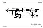

The front panel external ALC input goes via the A20
Motherboard PCB to the A10 ALC PCB; the rear
panel external ALC input goes by way of the A21-1/
A21-2 PCB and the A20 PCB to the A10 PCB. The
rear panel connectors,
10 MHz REF OUT
and
10 MHz REF IN
, are coupled directly to the A3 Refer-
ence Loop PCB via coaxial cables. The rear panel
IEEE-488 GPIB
and
SERIAL I/O
connectors are
connected to the A17 CPU PCB by way of the Moth-
erboard PCB.
In 691XXB models, the front panel AM and Square
Wave inputs go by way of the Motherboard PCB to
the internal PCBs—the AM input to the A10 ALC
PCB and the Square Wave input to the A9 PIN Con-
trol PCB. The rear panel AM and Square Wave
inputs route via the A21-2 PCB and the Mother-
board PCB to their respective internal PCBs. The
front panel and rear panel FM inputs are coupled
directly via coaxial cable to the A11 FM PCB.
Motherboard/
Interconnec-
tions
The A20 Motherboard PCB and associated cables
provide the interconnections for the flow of data,
signals, and DC voltages between all internal com-
ponents and assemblies throughout the 690XXB/
691XXB.
2-3
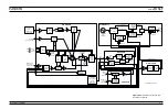
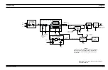
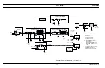
FREQUENCY SYNTHESIS
The frequency synthesis subsystem provides phase-lock control of the
690XXB/691XXB output frequency. It consists of four phase-lock loops,
the Reference Loop, the Coarse Loop, the Fine Loop, and the YIG
Loop. The four phase-lock loops, operating together, produce an accu-
rately synthesized, low-noise RF output signal. Figure 2-2 (page 2-11)
is an overall block diagram of the frequency synthesis subsystem. The
following paragraphs describe phase-lock loops and the overall opera-
tion of the frequency synthesis subsystem.
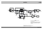
Phase Lock
Loops
The purpose of a phase-lock loop is to control the
frequency of a variable oscillator in order to give it
the same accuracy and stability as a fixed reference
oscillator. It works by comparing two frequency in-
puts, one fixed and one variable, and supplying a
correction signal to the variable oscillator to reduce
the difference between the two inputs. For example,
suppose we have a 10 MHz reference oscillator with
a stability of 1 x 10
-7
/day, and we wish to transfer
that stability to a voltage controlled oscillator
(VCO). The 10 MHz reference signal is applied to
the reference input of a phase-lock loop circuit. The
signal from the VCO is applied to the variable input.
690XXB/691XXB MM
2-9
FUNCTIONAL
FREQUENCY
DESCRIPTION
SYNTHESIS
Содержание 680 C Series
Страница 4: ......
Страница 5: ......
Страница 13: ...Figure 1 1 Typical Series 690XXB 691XXB Synthesized CW Signal Generator Model 69187B Shown ...
Страница 61: ......
Страница 97: ......
Страница 205: ......
Страница 207: ......
Страница 221: ......
Страница 225: ......
Страница 241: ......
Страница 259: ......
Страница 275: ......
Страница 285: ......
Страница 289: ......
Страница 299: ......
Страница 303: ......
Страница 315: ......


