background image

1

DEMO MANUAL DC2529A

UG-1311 Rev 0

For more information 

www.analog.com

Document Feedback

DESCRIPTION

LTC7810ELXE

High Input Voltage Dual Output 

Synchronous Buck Converter

Demonstration circuit 2529A is a dual output synchro-

nous buck converter featuring the LTC

®

7810ELXE in a 

48-lead eLQFP package. 
Key features of this board include: an optional on-board 

NMOS LDO for DRVCC; jumper for spread-spectrum 

option; optional resistors for single output dual phase 

operation; a mode selector that allows the converter to 

run in CCM, pulse-skipping, adjustable burst clamp or 

default Burst Mode

®

 operation; SYNC turret for Poly-

Phase

®

 operation.

L

, LT, LTC, LTM, Linear Technology, the Linear logo, Burst Mode and PolyPhase are registered 

trademarks of Analog Devices, Inc. All other trademarks are the property of their respective 

owners.

PERFORMANCE SUMMARY

The input voltage range of this demo board is from 16V to 

130V and it uses a sense resistor for overcurrent protec-

tion. The LTC7810 data sheet gives a complete descrip-

tion of the part, operation and application information and 

must be read in conjunction with this demo manual for 

DC2529A.

Design files for this circuit board are available at  

http://www.analog.com/DC2529A

Specifications are at T

A

 = 25°C

Table 1.  

PARAMETER

CONDITIONS

VALUE

Input Voltage Range

16V to 130V

Output Voltage V

OUT1

V

IN

 = 16V to 130V, I

OUT1

 = 0A to 10A, JP4: FCM

5V ± 2%

Output Voltage V

OUT2

V

IN

 = 16V to 130V, I

OUT2

 = 0A to 5A, JP4: FCM

12V ± 2% 

Maximum Output Current I

OUT1,MAX

V

IN

 = 16V to 130V, I

OUT1,MAX

10A

Maximum Output Current I

OUT2,MAX

V

IN

 = 16V to 130V, I

OUT2,MAX

5A

Default Operating Frequency (Typical)

100kHz

External Clock Sync. Frequency Range

75kHz to 750kHz

Typical Full Load Efficiency (See Figure 4)

V

IN

 = 48V, V

OUT1

 = 5V, I

OUT1

 = 10A  

V

IN

 = 48V, V

OUT2

 = 12V, I

OUT

 = 5A

88.7% 

95.4%

Содержание LTC7810ELXE

Страница 1: ...property of their respective owners PERFORMANCE SUMMARY The input voltage range of this demo board is from 16V to 130V and it uses a sense resistor for overcurrent protec tion The LTC7810 data sheet gives a complete descrip tion of the part operation and application information and must be read in conjunction with this demo manual for DC2529A Design files for this circuit board are available at ht...

Страница 2: ... FCM JP5 ON JP6 ON 2 With power off connect the input power supply to VIN and GND 3 Turn on the power at the input NOTE Make sure that the input voltage is higher than 16V and does not exceed 130V 4 Check the output voltages The output voltages should be within the specifications in Table 1 Once the proper output voltages are established adjust the load within the operating range and observe the o...

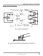
Страница 3: ...nformation www analog com Figure 1 Proper Measurement Equipment Setup QUICK START PROCEDURE Figure 2 Measuring Input or Output Ripple Across Terminals or Directly Across Ceramic Capacitor VOUT GND COUT VIN SUPPLY IIN LOAD IOUT LOAD DC2529A F01 IOUT ...

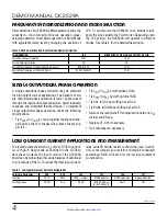
Страница 4: ...f Table 2 Mode Selection and Synchronized Operation Options CONFIGURATION JP4 MODE WITH SYNC SIGNAL APPLIED TO PLLIN Forced Continuous Operation FCM FCM Pulse Skipping Operation P S P S Burst Mode Operation with Adjustable Clamp Level BURST ADJ FCM Burst Mode Operation with Default Clamp BURST DEFAULT FCM JP4 To synchronize the DC2529A to an external clock apply the sync signal to the PLLIN turret...

Страница 5: ...VIN 24V VIN 48V VIN 72V VIN 100V VIN 130V IOUT A 0 1 2 3 4 5 60 65 70 75 90 100 95 80 85 EFFICIENCY DC2629A F04 VIN 24V VIN 48V VIN 72V VIN 100V VIN 130V 100µs DIV VOUT1 20MHz BW 50mV DIV DC2629A F05 100µs DIV VOUT2 20MHz BW 50mV DIV DC2629A F06 Figure 4 DC2529A VOUT2 Typical FCM Efficiency vs Load Current Figure 5 DC2529A VOUT1 2 5A to 5A Load Transient at VIN 48V Figure 6 DC2529A VOUT2 1 25A to ...

Страница 6: ...6 DEMO MANUAL DC2529A UG 1311 Rev 0 For more information www analog com Figure 7 Thermal Image VIN 130V VOUT1 5V at 10A VOUT2 12V at 5A No Air Flow TA 25 C ...

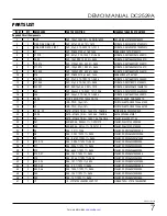
Страница 7: ...10 0603 MURATA GRM188R71C334KA01D 16 2 D3 D4 DIODE SCHOTTKY 150V SOD 123 CENTRAL SEMI CMHD3595 TR 17 1 L1 IND PWR 15µH 15 WURTH ELEKTRONIK 7443631500 18 1 L2 IND PWR 47µH 15 WURTH ELEKTRONIK 7443634700 19 3 Q1 Q3 Q7 XSTR MOSFET N CH 150V 21A TDSON 8 INFINEON BSC520N15NS3G 20 2 Q2 Q4 XSTR MOSFET N CH 150V 56A TDSON 8 BSC160N15NS5ATMA1 21 1 Q9 XSTR MOSFET N CH 150V 1 5A TDSON 8 VISHAY SI3440DV T1 E3...

Страница 8: ...030000Z0EA 7 0 R6 R7 R16 R17 R26 R27 R31 R33 R37 R41 R45 RES OPTION 0603 OPT 8 0 R39 RES OPTION 0805 OPT Hardware For Demo Board Only 1 9 E1 E9 TEST POINT TURRET 094 MTG HOLE MILL MAX 2501 2 00 80 00 00 07 0 2 6 J1 J2 J3 J4 J5 J6 CONN BANANA JACK KEYSTONE 575 4 3 1 JP1 HEADER 1 4 2MM WURTH ELEKTRONIK 62000411121 4 2 JP2 JP3 HEADER 1 3 2MM WURTH ELEKTRONIK 62000311121 5 1 JP4 HEADER 2 4 2MM WURTH E...

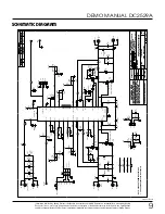
Страница 9: ... com 3 DEMO CIRCUIT 2529A Thursday June 29 2017 1 1 HIGH INPUT VOLTAGE DUAL OUTPUT N A LTC7810ELXE DING L SIZE DATE IC NO REV SHEET OF TITLE APPROVALS PCB DES APP ENG TECHNOLOGY Fax 408 434 0507 Milpitas CA 95035 Phone 408 432 1900 1630 McCarthy Blvd LTC CONFIDENTIAL FOR CUSTOMER USE ONLY CUSTOMER NOTICE LINEAR TECHNOLOGY HAS MADE A BEST EFFORT TO DESIGN A CIRCUIT THAT MEETS CUSTOMER SUPPLIED SPEC...

Страница 10: ...on of ADI Customer may not disclose or transfer any portion of the Evaluation Board to any other party for any reason Upon discontinuation of use of the Evaluation Board or termination of this Agreement Customer agrees to promptly return the Evaluation Board to ADI ADDITIONAL RESTRICTIONS Customer may not disassemble decompile or reverse engineer chips on the Evaluation Board Customer shall inform...

Отзывы: