


UG-1828
Preliminary Technical Data
Rev. PrC | Page 300 of 338
•
TX supports I/Q, I/Q FM/FSK, Direct FM/FSK types
•
Frequency Deviation
•
This option is available only for TX FM type setups.
•
ORx1 and ORx2 can be enabled for IQ input
•
Interface Rate allows the user to select the rate for the interface, this can be used to over or under sample from the sample rate. The
user may need to provide their own PFIR to account for this.
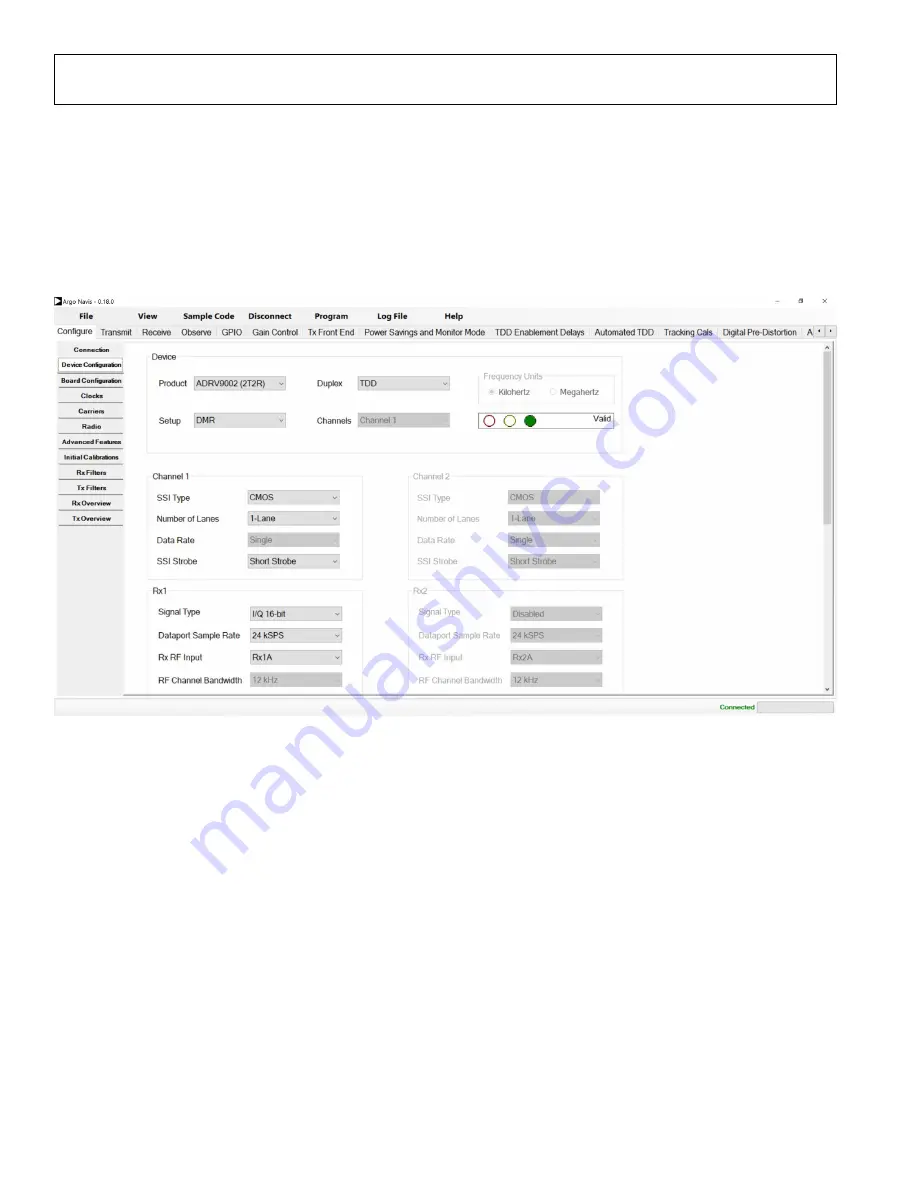
There is a traffic light indicator that checks the settings selected by the user and indicates if the settings are acceptable or not.
Figure 279. Device Configuration Tab
In the
Board Configuration
tab, there are settings for transmitter
External Loopback
. This is typically used for DPD type applications.
The user can either enable and disable the external loopback after power amplifier. If it is enabled, the user should enter the expected
loopback peak power in the
Peak Power
entry. Default peak power is −18 dBm. These are associated with RX1/2B ports.
The external loopback path delay can be measured using API, sending a low level wideband signal in the datapath for delay measurement.
This action disrupts transmit signal in the air. User should do this in a test environment and before the power amplifier is transmitting
real data. The user can use the ExternalPathDelay_Calibrate() and ExternalPathDelay_Get() to retrieve the external loopback path delay
in ns. There is an IronPython example of this available in the SDK, for details see IronPython Scripting section below. Note that for this
measurement there is a limitation with external delay measurement used by DPD.
1.
Measurement with LTE10 profiles is recommended to obtain the highest possible measurement accuracy.
2.
Customer should only make the measurement upon Navassa entering CALIBRATED state for the first time.
SSI Ref Clock
can be obtained from the Tx channel or the Rx channel. When using the clock from the Tx channel this will be pushed to
two GPIO pins. Using the Rx SSI clock releases these two pins for other uses.
External LNA
is used to control the analog output from GPIOs to control the gain of the system LNA. The pin settings currently are
locked to one nibble. Filling in the LNA gain steps will allow the API functions to calculate extra gain table settings. This can be seen in
the Gain Control Tab after you have programmed the part.
The Gain Table will now be extended with gain settings that include the user defined LNA configuration. The Extended Gain Control
column will specify the control word for the LNA and this is shown with colored backgrounds. The Duplicates column shows the row


