ADM1060
Rev. B | Page 33 of 52
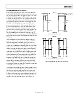
OUTPUTS
PROGRAMMABLE DRIVER OUTPUTS
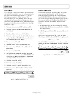
The ADM1060 has nine programmable driver outputs (PDOs).
These are the logic outputs of the device. Each PDO is normally
controlled by a single PDB. Thus, the PDOs can be set up to
assert when the conditions on the PDB are met, such as when
the SFDs are in tolerance, the levels on the GPI are correct, the
watchdog timer has not timed out, and so on. The PDOs can be
used for a number of functions; for example, to provide a
POWER_GOOD signal when all the SFDs are in tolerance, pro-
vide a reset generator output if one of the SFDs goes out of spec
(which can be used as a status signal for a DSP or other micro-
processor), or provide enable signals for LDOs on the supplies
that the ADM1060 is supervising.
There are a number of pull-up options on the PDOs to enable
the user to program the output level.
The outputs can be programmed as
•
Open-drain (allows the user to connect an external pull-up
resistor)
•
Open-drain with weak pull-up to V
DD
•
Push-pull to V
DD
•
Open-drain with weak pull-up to VPn
•
Push-pull to VPn
•
Internally charge-pumped high drive (12 V)
The last option is only available on PDO1−4. This allows the
user to directly drive the gate of an N-channel FET in the path
of a power supply. The required pull-up is selected by pro-
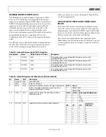
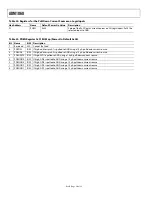
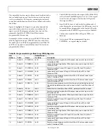
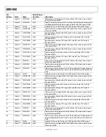
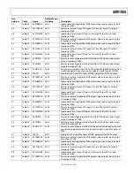
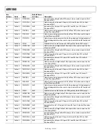
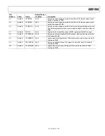
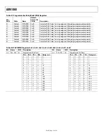
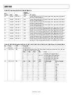
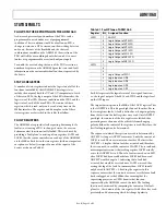
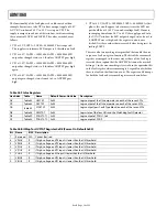
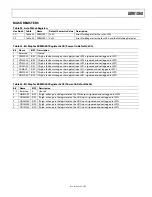
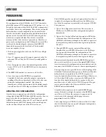
gramming Bits 0 to 3 in PnPDOCFG appropriately (see
Table 40).
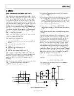
The data driving each of the PDOs can come from one of three
inputs. These inputs are enabled by a bit each in the
PnPDOCFG registers. The inputs are
•
The (delayed) output from the associated PLB (enabled by
setting bit CFG4 to 1)
•
Data that is driven directly over the SMBus interface (enabled
by setting Bit CFG5 to 1). When set in this mode, the data
from the PDB is disabled and the data on the PDO is the data
on CFG4. Thus, the PDO can be software controlled to initi-
ate a software power-up/power-down.
•
An on-chip clock (enabled by setting Bit CFG6 to 1). A
100 kHz clock is available to clock an external device such as
an LED.
More details on these data modes are given in the register map
of Table 40.
The default setup of each of the PDOs is to be pulled low by a
weak (20 kΩ) pull-down resistor. This is also the setup of the
PDOs on power-up until the registers are loaded and the pro-
grammed conditions are latched. The outputs are actively
pulled low once 1 V or greater is seen at any VPn or VH. Until
there is a 1 V supply on the chip, the outputs are high imped-
ance. This provides a known condition for the PDOs during
power-up. The internal pull-down can be overdriven with an
external pull-up of suitable value tied from the PDO pin to the
required pull-up voltage. The 20 kV resistor must be accounted
for in calculating a suitable value. For example, if it is required
to pull PDOn up to 3.3 V, and 5 V is available as an external
supply, the pull-up resistor value is given by:
3.3
V
= 5
V
× 20
kV
/(
R
UP
+ 20
kV
)
Therefore,
R
UP
=
(100
kV
– 66
kV
)/3.3 = 10
kV
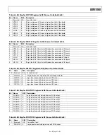
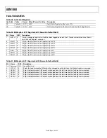
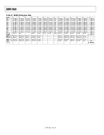
The register list and the bit map for the PDOs are shown in
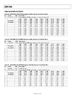
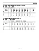
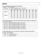
Table 39 and Table 40.
CF
G4
CF
G5
CF
G6
PDB_OUT
CFG4
M_CLK
SEL
VP1
VP4
V
DD
VFET (PDO1
–4 ONLY)
PDO
20k
Ω
10
Ω
20k
Ω
10
Ω
20k
Ω
10
Ω
20k
Ω
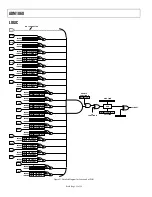
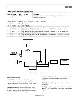
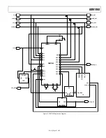
Figure 23. Programmable Driver Output
Содержание ADM1060
Страница 51: ...ADM1060 Rev B Page 51 of 52 NOTES ...

