background image

ADM-VPX3-9Z2 User Manual

V1.1 - 16th January 2020

3.5.1 IO Delay Reference Clock (FABRIC_CLK)

The fixed reference clock FABRIC_CLK is a differential LVDS signal.

FABRIC_CLK is used as the reference clock for the IO delay control block (IDELAYCTRL).

Signal

Frequency

Target FPGA Input

IO Standard

"P" pin

"N" pin

FABRIC_CLK

300 MHz

IO BANK 47

LVDS

G21

F21

Table 9 : DDR REFCLK Connections

3.5.2 Fixed 100MHz Reference clock REFCLK100M

A fixed 100MHz reference clock is available on the board.

Signal

Frequency

Target FPGA Input

IO
Standard

"P" pin

REFCLK100M[0]

100 MHz

PS_505_MGTREFCLK_0 LVDS

AA27

REFCLK100M[1]

100 MHz

IO BANK 48

LVDS

E17

REFCLK100M[2]

100 MHz

MGTREFCLK1_230

LVDS

B10

REFCLK100M[3]

100 MHz

MGTREFCLK1_128

LVDS

N27

Table 10 : REFCLK100M Connections

3.5.3 Programmable Clocks (PROGCLK1 and PROGCLK2)

There are two programable clock sources that are forwarded throughout the FPGA. These clocks can be

programmed via the avr2util utility contained within the Alpha Data ADM-VPX3-9Z2 SDK. PROGCLK1 and

PROGCLK2 are generated by a dedicated programmable clock generator IC and offer extremely high frequency

resolutions (1ppm increments).

Signal

Frequency

Target FPGA Input

IO Standard

"P" pin

"N" pin

PROGCLK1[0]

5 - 400 MHz

PS_505_MGTREFCLK_1 LVDS

W27

W28

PROGCLK1[1]

5 - 400 MHz

IO BANK 67

LVDS

R10

R9

PROGCLK1[2]

5 - 400 MHz

MGTREFCLK1_228

LVDS

J8

J7

PROGCLK1[3]

5 - 400 MHz

MGTREFCLK1_129

LVDS

J27

J28

Table 11 : PROGCLK1 Connections

Note: PROGCLK1[3:0] are all buffered copies of the same clock signal.

Signal

Frequency

Target FPGA Input

IO Standard

"P" pin

"N" pin

PROGCLK2[0]

5 - 400 MHz

IO BANK 48

LVDS

E19

D19

PROGCLK2[1]

5 - 400 MHz

IO BANK 64

LVDS

AK8

AK7

PROGCLK2[2]

5 - 400 MHz

MGTREFCLK1_130

LVDS

E27

E28

PROGCLK2[3]

5 - 400 MHz

MGTREFCLK1_229

LVDS

E8

E7

Table 12 : PROGCLK2 Connections

Note: PROGCLK2[3:0] are all buffered copies of the same clock signal.

Page 12

Functional Description

ad-ug-1323_v1_1.pdf

Содержание ADM-VPX3-9Z2

Страница 1: ...ADM VPX3 9Z2 User Manual Document Revision 1 1 16th January 2020...

Страница 2: ...or form without prior written consent from Alpha Data Parallel Systems Ltd Head Office Address Suite L4A 160 Dundee Street Edinburgh EH11 1DQ UK Telephone 44 131 558 2600 Fax 44 131 558 2700 email sa...

Страница 3: ...IO Delay Reference Clock FABRIC_CLK 12 3 5 2 Fixed 100MHz Reference clock REFCLK100M 12 3 5 3 Programmable Clocks PROGCLK1 and PROGCLK2 12 3 5 4 Module to Carrier Global Clocks CLK_M2C 13 3 5 5 Module...

Страница 4: ...Definitions 8 Table 9 DDR REFCLK Connections 12 Table 10 REFCLK100M Connections 12 Table 11 PROGCLK1 Connections 12 Table 12 PROGCLK2 Connections 12 Table 13 CLK_M2C Connections 13 Table 14 GCLK_M2C...

Страница 5: ...of Figures Figure 1 ADM VPX3 9Z2 Air Cooled 4 Figure 2 ADM VPX3 9Z2 Block Diagram 5 Figure 3 LED Locations 7 Figure 4 JTAG Boundary Scan Chain 10 Figure 5 Clocks 11 Figure 6 Ethernet Interfaces 15 Fig...

Страница 6: ...ADM VPX3 9Z2 User Manual V1 1 16th January 2020 Page Intentionally left blank...

Страница 7: ...lane PCI Express Gen 2 interface on the OpenVPX Data Plane 3 lanes on the OpenVPX Expansion Plane and 1 lane to an on board SSD drive chip 1 lane of PCIe on the Data Plane 2 lanes on the Expansion Pl...

Страница 8: ...1 References 1 3 Order Code ADM VPX3 9Z2 z 2 c o Name Symbol Configurations Zynq Ultrascale device z 15EG ZU15EG 9EG ZU9EG Contact factory for details Cooling c blank air cooled commercial AC1 air coo...

Страница 9: ...s highly dependent on the FPGA application A power estimator spreadsheet is available on request from Alpha Data This should be used in conjunction with Xilinx power estimation tools to determine the...

Страница 10: ...2 3 Software Installation Please refer to the Reference Designs on the Alpha Data Download Site Example projects for configuring the Zynq Ultrascale MPSOC device and example software for running on t...

Страница 11: ...ADM VPX3 9Z2 User Manual V1 1 16th January 2020 3 Functional Description 3 1 Overview Figure 2 ADM VPX3 9Z2 Block Diagram Page 5 Functional Description ad ug 1323_v1_1 pdf...

Страница 12: ...connected to PS HSSIO lane 1 SW3 4 Flash Boot Inhibit Target FPGA is not configured from onboard flash memory Target FPGA is configured from on board flash memory SW3 5 VPX JTAG Connect JTAG chain to...

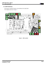
Страница 13: ...Definitions There are seven LEDs to provide a visual indication of the board status Their locations are shown in Figure 3 D5 D11 D6 D7 D10 D8 D9 D12 D15D14 D13 D18 D17 D16 D19 D22 D21 Figure 3 LED Lo...

Страница 14: ...efinitions A further two sets of three LEDs provide an indication of the status of the two Ethernet interfaces Comp Ref Function ON State Off State D9 Green Ethernet 0 LED0 See Table 19 D8 Green Ether...

Страница 15: ...C pin E22 AUXCLK_N is connected to FPGA GC pin D22 3 2 3 REFCLK Reference Clock This clock is an input to the onboard clock distribution and generation system The 50MHz defined in OpenVPX can be used...

Страница 16: ...ON header J2 should not be used 3 4 2 VPX Interface The JTAG interface on the VPX backplane is normally unused When SW3 5 is OFF default all JTAG signals to P0 are left floating The JTAG interface can...

Страница 17: ...given in Clocks A description of each clock follows Zynq Ultrascale MGT Banks MGT130 REFCLK0 REFCLK1 MGT129 REFCLK0 REFCLK1 MGT128 REFCLK0 REFCLK1 MGT230 REFCLK0 REFCLK1 MGT229 REFCLK0 REFCLK1 MGT228...

Страница 18: ...that are forwarded throughout the FPGA These clocks can be programmed via the avr2util utility contained within the Alpha Data ADM VPX3 9Z2 SDK PROGCLK1 and PROGCLK2 are generated by a dedicated progr...

Страница 19: ...an MGTREFCLK input on the FPGA Signal Frequency FPGA Input IO Standard P pin N pin GBTCLK_0_M2C Variable MGTREFCLK_228 LVDS L8 L7 GBTCLK_1_M2C Variable MGTREFCLK_229 LVDS G8 G7 GBTCLK_2_M2C Variable...

Страница 20: ..._POR_B pin Clears all logic Mode pins sampled i e reconfigures hardware Reboots MPSoC SW2 Soft Reset PS_SRST_B pin Same as Power on Reset but does not sample Mode pins hardware configuration unchanged...

Страница 21: ...nnected to the PS via RGMII The Zynq PS MDIO interface is also connected to the VPX connector via buffers VPX P1 PHY SGMII_1 RGMII_1 PS PHY SGMII_0 RGMII_0 ETH0 ETH1 Buffers MDIO MDC MDIO MDC Figure 6...

Страница 22: ...heir voltage and function are shown in PL FPGA IO Banks IO Banks Voltage Purpose 65 66 67 FMC_VADJ FMC GPIO LA and HA 64 FMC_VIO_B FMC GPIO HB 25 46 47 FMC3_VADJ FMC GPIO 47 48 2 5V VPX P2 GPIO 50 3 3...

Страница 23: ...Regional Clock GPIO pair 2 single ended HB_CC 6 Regional Clock GPIO pair 2 single ended HB_CC 17 Regional Clock GPIO pair 2 single ended Table 22 FMC Groups J1 3 8 4 VPX P2 GPIO Interface The P2 VPX...

Страница 24: ...e being operated within the specified limits If the temperature is close to the limit a Warning Alarm interrupt is set If a limit is exceeded a Critical Alarm interrupt is set After the Critical Alarm...

Страница 25: ...rmance and flexible front panel interface through a range of interchangeable industry standard IO modules which connect at receptacle J1 The FMC interface adheres to VITA 57 4 The ADM VPX3 9Z2 utilize...

Страница 26: ...ADM VPX3 9Z2 User Manual V1 1 16th January 2020 Page Intentionally left blank Page 20 Functional Description ad ug 1323_v1_1 pdf...

Страница 27: ...P D3 W31 Y33 A3 PCIE_RX2_P PCIE_TX2_N E3 W32 Y34 B3 PCIE_RX2_N PCIE_TX3_P E4 V29 V33 B4 PCIE_RX3_P PCIE_TX3_N F4 V30 V34 C4 PCIE_RX3_N Table 27 Data Plane P1 Wafers 1 4 Appendix A 2 Data Expansion Pla...

Страница 28: ..._2 D13 B29 C31 A13 P1_MUX_RX_P_2 P1_MUX_TX_N_2 E13 B30 C32 B13 P1_MUX_RX_N_2 P1_MUX_TX_P_3 E14 A31 B33 B14 P1_MUX_RX_P_3 P1_MUX_TX_N_3 F14 A32 B34 C14 P1_MUX_RX_N_3 Table 29 Expansion User Plane P1 Wa...

Страница 29: ...7_N GP1_P E6 J17 C18 D3 GP7_P GP2_N C6 K17 B19 B3 GP8_N GP2_P B6 L17 B18 A3 GP8_P GP3_N E5 K18 C22 F2 GP9_N GP3_P D5 L18 D21 E2 GP9_P GP4_N B5 H19 B21 C2 GP10_N GP4_P A5 H18 C21 B2 GP10_P GP5_N F4 C17...

Страница 30: ...LA05_P D11 W5 L16 E6 HA05_P LA06_N C11 W6 N8 K11 HA06_N LA06_P C10 W7 N9 K10 HA06_P LA07_N H14 U4 K12 J10 HA07_N LA07_P H13 U5 L12 J9 HA07_P LA08_N G13 AB5 L11 F11 HA08_N LA08_P G12 AB6 M11 F10 HA08_P...

Страница 31: ...A22_P LA23_N D24 AH11 Y9 K23 HA23_N LA23_P D23 AH12 Y10 K22 HA23_P LA24_N H29 AJ2 AL7 K26 HB00_CC_N LA24_P H28 AH2 AL8 K25 HB00_CC_P LA25_N G28 AJ1 AM11 J25 HB01_N LA25_P G27 AH1 AL11 J24 HB01_P LA26_...

Страница 32: ...1_N E37 AP3 AP7 J34 HB15_N HB21_P E36 AN3 AN7 J33 HB15_P FMC_CLK_DIR B1 V9 Table 32 GPIO Pins Appendix C 2 Clock Pins Signal FMC J1 FPGA FPGA FMC J1 Signal CLK0_M2C_N H5 AA5 AG6 K5 CLK2_BIDIR_N CLK0_M...

Страница 33: ...5 B33 DP7_C2M_N DP7_M2C_P B12 F2 F6 B32 DP7_C2M_P DP8_M2C_N B9 D1 E3 B29 DP8_C2M_N DP8_M2C_P B8 D2 E4 B28 DP8_C2M_P DP9_M2C_N B5 C3 D5 B25 DP9_C2M_N DP9_M2C_P B4 C4 D6 B24 DP9_C2M_P DP10_M2C_N Y11 B1...

Страница 34: ...DP19_M2C_N M7 C32 B30 Z5 DP19_C2M_N DP19_M2C_P M3 B34 A32 Y3 DP19_C2M_P DP20_M2C_N Z32 L31 K29 M26 DP20_C2M_N DP20_M2C_P Y34 K33 J31 M30 DP20_C2M_P DP21_M2C_N Z36 H33 H29 M34 DP21_C2M_N DP21_M2C_P Y38...

Страница 35: ...Manual V1 1 16th January 2020 Revision History Date Revision Nature of Change 21 Sep 2018 0 1 Initial Draft 02 Jan 2020 1 0 First Release 16 Jan 2020 1 1 Added pinout tables Page 29 Revision Table ad...

Страница 36: ...dee Street Edinburgh EH11 1DQ UK Telephone 44 131 558 2600 Fax 44 131 558 2700 email sales alpha data com website http www alpha data com Address 611 Corporate Circle Suite H Golden CO 80401 Telephone...

Отзывы: