ADM-PCIE-9V5 User Manual
3.9 GPIO Connector
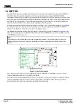
The GPIO option consists of a versatile shrouded connector from Molex with part number 87832-1222. This
connector gives users eight signals connected to the FPGA.
Recommended mating plug: Molex 0875681273 or 0511101260
Figure 14 : GPIO Connector Schematic
Figure 15 : GPIO Connector Location
3.9.1 Direct Connect FPGA Signals
8 nets are broken out to the GPIO header, as four sets of differential pairs. These signal are suitable for any 1.8V
signalling standards supported by the Xilinx UltraScale architecture. See Xilinx UG571 for IO options. LVDS and
1.8 CMOS are popular options. The 0th GPIO signal index is suitable for a global clock connection.
The direct connect GPIO signals are limited to 1.8V by a quickswitch (74CBTLVD3245PW) in order to protect the
FPGA from overvoltage on IO pins. This quickswitch allows the signals to travel in either direction with only 4
ohms of series impedance and less than 1ns of propagation delay. The nets are directly connected to the FPGA
after the quickswitch.
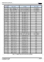
Direct connect signal names are labeled GPIO_0_1V8_P/N and GPIO_1_1V8_P/N, etc. to show polarity and
grouping. The signal pin allocations can be found in
3.9.2 Timing Input
Pins 1 and 2 of J1 can be used as an isolated timing input signal (up to 25MHz). Applications can either directly
connect to the GPIO connector, or Alpha Data can provide a cabled solution with an SMA or similar connector on
Page 20
Functional Description
ad-ug-1385_v1_0.pdf


