ADM-PCIE-8K5-FH User Manual
3.8 SMA Timing Input
All cards are fitted with a U.FL connector that can be utilized as a timing input. This connector can be accessed
with a U.FL cable internal to the chassis, or cabled to an SMA or similar connector at the front panel. Contact
[email protected] for front panel connector options.
Input is on FPGA pin AL30, IOSTANDARD LVCMOS18
The signal is isolated through a optical isolator part number ACPL-M61L with a 739 ohm of series resistance.
Figure 10 : Timing Input Schematic
3.9 USB Front Panel Interface
The ADM-PCIE-8K5-FH houses two USB ports. The upper connector connects to the system monitor system,
while the lower connector allows programming of the FPGA.
For convenience the FPGA can be configured directly from the lower USB connection on the front panel. The
ADM-PCIE-8K5-FH utilizes the Digilent USB-JTAG converter box which is supported by the Xilinx software tool
suite. Simply connect a micro-USB AB type cable between the upper ADM-PCIE-8K5-FH USB port and a host
computer with Vivado installed. Vivado Hardware Manager will automatically recognize the FPGA and allow you
to configure the FPGA and the BPI configuration PROM.
The upper USB connector is used to directly access the system monitor system. All voltages, currents,
temperatures, and non-volatile clock configuration settings can be accessed using Alpha Data's avr2util software
at this interface.
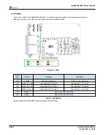
The location of the upper (J11) and lower (J15) ports are clarified in the diagram below.
Figure 11 : SFP Locations
Avr2util is downloadable here:
Page 15
Functional Description
ad-ug-1342_v1_0.pdf


