ADM-PCIE-8K5-FH User Manual
Signal
Target FPGA Input
I/O Standard
pin
FABRIC_CLK
IO_L12P_T1U_GC_64
LVCMOS33
AM19
Table 6 : Fabric Clock
3.2.3 Programming Clock (EMCCLK)
An 100MHz clock is fed into the EMCCLK pin to drive the BPI flash device during configuration of the FPGA.
Signal
Target FPGA Input
I/O Standard
pin
REFCLK100M
IO_L24P_T3U_N10_EMCCLK_65
LVCMOS18
AJ28
Table 7 : EMCCLK
3.2.4 SFP+
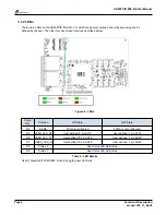
This board houses two 2x1 SFP+ cages, allowing for four total connections. Connectors SFP0 and SFP1 are
located in MGT tile 227, while connectors SFP2 and SFP3 are located in MGT tile 228. See
SFP+
for information
on connector locations. Each of the 2x1 SFP+ cages has its own unique clock source. Both clocks are initially set
to 156.25MHz. Note that these clock frequency can be changed to any arbitrary clock frequency up to 312.5MHz
by re-programing the Si5338 reprogrammable clock oscillator via system monitor. This can be done using the
Alpha Data API or over USB with the appropriate Alpha Data Software tools. Any changes made to the default
clock frequency are non-volatile and will be used moving forward.
Signal
Target FPGA Input
I/O Standard
"P" pin
"N" pin
GTH_CLK_0
MGTREFCLK0_227
LVDS
AE8
AE7
GTH_CLK_1
MGTREFCLK0_228
LVDS
AA8
AA7
SI5328_REFCLK_OUT0
MGTREFCLK1_228
LVDS
W8
W7
Table 8 : SFP+ Reference Clocks
The SFP+ cages are also located such that they can be clocked from a Si5328 jitter attenuator clock multiplier. If
jitter attenuation is required please see the reference documentation for the Si5328. https://www.silabs.com/
Support%20Documents/TechnicalDocs/Si5328.pdf
The Si5328 is configured with a 114.285MHz oscilator on XA and XB, SDA is at FPGA pin L29 (1.8V), SCL is at
FPGA pin L30 (1.8V) with external pull-ups included.
The Si5328 input clock comes from FPGA pins M29 and M30, and includes 100 Ohm AC coupled termination on
the 1.8V FPGA bank.
The Jitter Attenuator is not fitted by default and requires a custom bulid option. Contact [email protected]
for more details.
3.2.5 FireFly
The two optional FireFly sites are located in MGT tile 231 and 232 and can use a variety of reference clocks.
PCIE_REFCLK_1 is a buffered version of the PCIe edge clock. It is converted to LVDS through a NB6L11S clock
buffer.
GTH_CLK_2 is default to 156.25MHz. Note that these clock frequency can be changed to any arbitrary clock
frequency up to 312.5MHz by re-programing the Si5338 reprogrammable clock oscillator via system monitor.
This can be done using the Alpha Data API or over USB with the appropriate Alpha Data Software tools. Any
changes made to the default clock frequency are non-volatile and will be used moving forward.
EXT_CLK comes from the GPIO header. The signal is fed directly to the GTH clock with only 10nF capacitors in
Page 8
Functional Description
ad-ug-1342_v1_0.pdf


