


5-14
Service Guide E8364-90026
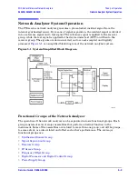
Theory of Operation
PNA Series Microwave Network Analyzers
Source Group Operation
E8362B, E8363B, E8364B
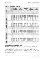
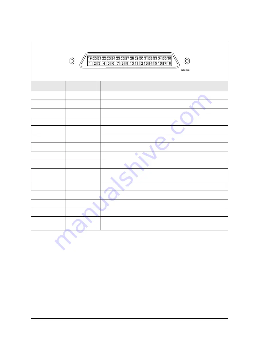
Table 5-4
HANDLER I/O Connector Key Pin Assignments
Rectangular 36-Pin Female Connector
Pin Numbers
Name
Function
1
GND
0 V, ground reference
2
INPUT1
TTL in, negative pulse (1
μ
s min) latches OUTPUT1-2
3–4
OUTPUT1–2
TTL out, latched
5–12
Port A0–7 Out
TTL out, latched
13–20
Port B0–7 Out
TTL out, latched
21–24
Port C I/O
TTL I/O, latched
25–28
Port D I/O
TTL I/O, latched
29
Port C Status
TTL out, low = input mode, high = output mode
30
Port D Status
TTL out, low = input mode, high = output mode
31
Output Strobe
Write Strobe
TTL out, active low data write strobe (1
μ
s min)
32
No connect
Not used
33
Pass Fail
TTL out, latched, indicates pass fail (programmable polarity)
34
+5 V
+5 Vdc, 100 mA max.
35
Sweep End
TTL out, active low (10
μ
s min) indicates sweep done
36
Pass/Fail
Write Strobe
TTL out, active low pass/fail write strobe (1
μ
s min)
Содержание E8362B
Страница 11: ...Service Guide E8364 90026 1 1 1 Safety and Regulatory Information ...
Страница 19: ...Service Guide E8364 90026 2 1 2 General Product Information ...
Страница 33: ...Service Guide E8364 90026 3 1 3 Tests and Adjustments ...
Страница 83: ...Service Guide E8364 90026 4 1 4 Troubleshooting ...
Страница 151: ...Service Guide E8364 90026 5 1 5 Theory of Operation ...
Страница 185: ...Service Guide E8364 90026 6 1 6 Replaceable Parts ...
Страница 269: ...Service Guide E8364 90026 7 1 7 Repair and Replacement Procedures ...
Страница 351: ...Service Guide E8364 90026 8 1 8 General Purpose Maintenance Procedures ...


