APDCAM User’s Guide
Page 1/32
APDCAM
Digital Avalanche Photodiode camera
User’s Guide
Version 1.01
Copyright © Adimtech Kft. 2010
Страница 1: ...APDCAM User s Guide Page 1 32 APDCAM Digital Avalanche Photodiode camera User s Guide Version 1 01 Copyright Adimtech Kft 2010 ...
Страница 2: ... 10 Controls and indicators 10 3 APDCAM Reference Manual 12 3 1 System Overview 12 3 2 Detector and analog electronics 13 3 3 Data Acquisition Unit 15 3 3 1 ADC Timing 18 3 3 2 Filtering resampling and channel selection 18 3 3 3 Triggering overload protection 21 3 3 4 Data output format 22 3 3 5 Offset control 22 3 4 Control unit 23 3 4 1 Detector bias voltage setting 23 3 4 2 Temperature control ...
Страница 3: ...ource The digital part of the camera contains individual Analog to Digital Converters for all 32 channels These ADCs continuously digitize data with 14 bit resolution and 10 50 MHz frequency The resulting data stream can be digitally filtered and downsampled in the camera to provide an output data stream with a frequency band matching the final sampling rate Various triggering and sampling schemes...
Страница 4: ...ptical interface Lens mount Nikon F mount Window material BK7 with antireflection coating Shutter Type Electromagnetically operated mechanical Control Software or external input Calibration light Type Red LED with fibre coupling Control DC set from software Sensitivity and noise Sensitivity Gain 100 14 bit mode2 2 4 106 photon s digit Noise equivalent photon flux no light2 Typical 5 107 photon s A...
Страница 5: ...t be significantly lower Data transmission Data and control interface Gigabit Ethernet over UTP and Fibre Communication format UDP both directions Fibre interface Multimode Duplex SC Max data rate 32 channels3 2 MHz 12bit Power input Power input 12 V DC max 6A Power connector on power supply Lemo FFA 0S 302 CLAK68 Mechanical Size L W H 36 16 19 cm Weight without power supply 6 7 kg ...
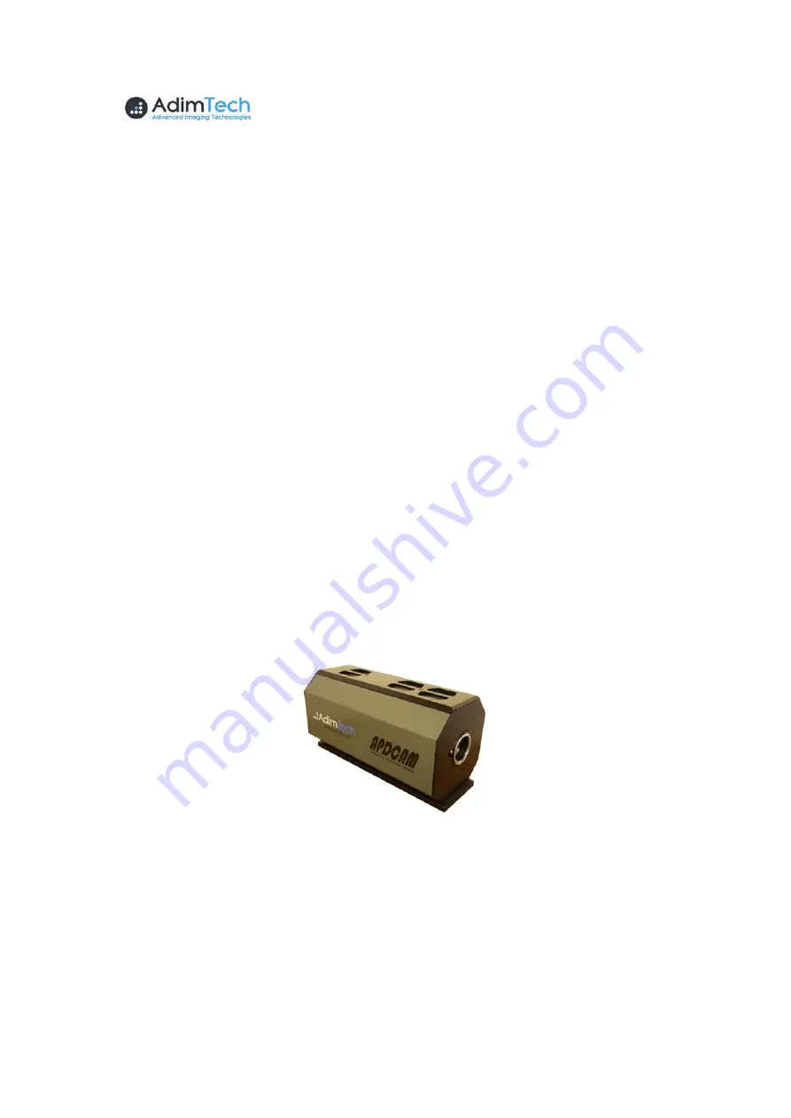
Страница 6: ...APDCAM User s Guide Page 6 32 F mount Fans Fibre converter Backplate with connectors and indicators Figure 1 View of APDCAM ...
Страница 7: ... desirable the fans can also be set to fixed speed 2 4 Configuration The operating parameters of APDCAM are set up in two internal register tables one for the data acquisition and one for the camera control Status of the camera can also be read from these registers Settings are stored in non volatile memory therefore after switching off and on the camera the setup will remain the same There are a ...
Страница 8: ...or the Gbit interface and register read write in one of the two internal modules of APDCAM the data acquisition module and the control module The camera may answer to these UDP datagrams by sending one ore more responding UDP datagrams For a standard setup the Gigabit interface parameters need not be modified For spe cial settings please consult the separate Gigabit interface documentation Additio...
Страница 9: ...otection against overload is provided by the digital electronics If en abled it can switch off the detector bias voltage when the signal level is above a certain limit over a predefined time In order to stabilise the gain the detector temperature should be kept constant This is accomplished by a temperature control circuit The standard detector temperature is 18 C which under normal room temperatu...
Страница 10: ...uartz oscillator However if needed this can be replaced by an external clock signal to provide strictly synchronous operation between several cameras or other devices 2 10 Controls and indicators APDCAM has several indicator LEDs and input output connectors mounted on its back plate Their function is described in Table 3 The photo of the backplate where these units are mounted is shown in Figure 3...
Страница 11: ... various internal sig nals in the factory Ethernet UTP connection to PC Optical Ethernet UTP UTP cable connection from Ethernet connector of APDCAM if fibre communication is desired Optical Ethernet fibre Fibre data connection to PC LEDs Temp Red light means temperature alarm Some element of the camera is overheated Overload Red light means overload condition occurred detector bias voltage is swit...
Страница 12: ...the detector via four optical fibres which illuminate the detector from 4 directions The detector bias voltage is also controlled digitally thus having the possibility of adjusting the detector gain to the re quirements The photocurrent from each of the 32 detector pixels is amplified by a sensitive low noise amplifier To compensate for the offset drift the output offset level of the amplifiers ca...
Страница 13: ...exact limit is dependent on the individual detector There is also a mini mum recommended detector bias voltage of 200 V below that the crosstalk through the pixels causes excessive noise The control card also controls the detector temperature by cooling or heating it via a Peltier element No computer intervention is needed for the control only parameters can be set from the PC Operation parameters...
Страница 14: ...The gain as a function of the applied voltage is shown together with the Quantum efficiency QE in Figure 6 Besides the gain the bias voltage also changes the detector capacitance it de creases with increasing voltage As all pixels are operated from a common bias voltage at low voltage setting the crosstalk increases between channels which results in an increase of the noise and its coherency betwe...
Страница 15: ...e causes higher gain Please consult the Hamamatsu S8550 datasheet for details The analog electronics utilize two amplifier stages for each channel their bandwidth is from DC to a maximum frequency Parameters of the first stage feedback resistor and capacitance determine the bandwidth and also the noise level For setting an optimal Signal to Noise ratio some information on the expected light level ...
Страница 16: ...irst Bit 7 Preamble enable ADC_PLL_MULT R W 12 1 EEPROM PLL multiplier for ADC clock generation Valid 20 50 ADC_PLL_DIV R W 13 1 EEPROM PLL divider for ADC clock generation Valid 8 100 STREAM_PLL_MULT R W 14 1 EEPROM PLL multiplier for ADC clock generation Valid 20 50 STREAM_PLL_DIV R W 15 1 EEPROM PLL divider for ADC clock generation Valid 8 100 STREAM_CTRL R W 16 1 0 The four lower bits enable t...
Страница 17: ...es are 500 1000 INT_TRIG_LEVEL R W 112 64 EEPROM 32x2 bytes internal trigger setting for each channel Bits 0 13 trigger level Bit 14 0 positive trigger level 1 negative trigger level Bit 15 Enable trigger from this channel ACT_SAMPLE R 176 16 0 4x4 byte indicating the number of acquired samples per stream As the sample timing is identical for all channels these values are nor mally identical OVERL...
Страница 18: ...Hz An additional limitation is that the base clock multiplied by ADC_PLL_MULT should be between 400 and 1000 MHz The status of the PLL units can be read from the STATUS1 and STATUS2 registers This is important especially if external clock is used The external clock PLL status is also shown on the camera backplate by the green Ext Clock LED The 8 channel ADC blocks have a built in test pattern gene...
Страница 19: ...lected cases in Table 7 Here the ADC frequency is assumed to be 10 MHz If a different ADC frequency is used all frequencies should be scaled proportionally Filter Coefficients COEFF_01 COEFF_08 fREC MHz fFIR MHz 01 02 03 04 05 06 07 08 50 0 5 0 00512 00000 00000 00000 00000 00000 00000 00009 50 0 2 0 00290 00202 00048 00000 00000 00000 00000 00009 50 0 1 0 00190 00164 00102 00042 00008 00000 00000...
Страница 20: ...hen all the channels are operating therefore some data reduction is needed This can be done either by reducing the number of active channels or by resampling the data decima tion to lower frequency Channels can be enabled individually see CH_ENABLE register Resampling can be done for all active channels in the same way The resampling clock can be either a divided version of the ADC clock see regis...
Страница 21: ... registers Triggering of data transmission can be achieved using several schemes External trigger Bit 0 or 1 of the TRIGGER register should be set and the TTL trigger signal connected to the Trigger In connector Depending on the bit set the trigger event happens on rising or falling edge Internal trigger This enables starting the data acquisition when the signal level in the detector channels is a...
Страница 22: ...e signal An overload event is generated when any of the signals fulfills the overload condition for more than OVERLD_TIME The overload event switches off the detector bias voltage and lits the red Overload LED on the backplate The status of the overload can be read from OVERLD_STATUS and writing any value into this register clears the overload The bias voltage should be switched back in the Contro...
Страница 23: ...amera back plate If the Control unit encounters a fatal problem this LED is red 3 4 1 Detector bias voltage setting In order to prevent accidental setting by e g software error the detector bias voltage is set in several steps First the required value is entered in the BIAS_SET register Please note the conversion factor The Control unit limits bias voltage to a maximum value BIAS_MAX set during fa...
Страница 24: ...d closes the shutter The drive electronics is not designed to open close the shutter at high frequency but it is intended for single open close cycles every few seconds as the shortest period time The shutter can be kept open or closed for any time When the shutter is open the yellow Shutter LED is lit on the camera backplate In SHUTTER_MODE 1 the shutter can be controlled externally by an electri...
Страница 25: ... 2 s complement 16 bit value represent ing the status of the Peltier cooler heater Nega tive values mean cooling positive heating The maximum is about 4000 PID_P R W 80 2 EEPROM Weights of the P I and D components of the detector temperature controller PID_I R W 82 2 EEPROM PID_D R W 82 2 EEPROM BIAS_SET R W 86 2 EEPROM The set value of the detector bias voltage The conversion factor is 0 12V digi...
Страница 26: ...smission to the PC the card can also communicate with the APDCAM DAQ and Control units on an internal bus and arrange register read write operations between the PC and APDCAM Communication on this internal bus is shown by blinking of the green Communication LED on the camera backplate Details of the GEC card are described in its own documentation The software interface description in Section 3 6 i...
Страница 27: ...ens communication with the camera close Closes communication with the camera writePDI Write one or more registers in one of the camera modules readPDI Read the contents of one or more registers in one of the cam era modules GetPdiIrqCount Return the number of interrupt UDP datagrams received SendTS Start data sending from the camera to the PC DontSendTS Stop sending data from the camera to the PC ...
Страница 28: ...ress 1 is for the DAQ module 2 is for the Control module subaddrss is the start address of the register which should be written while noofbytes is the number of bytes to be written and PData is the pointer to the data to be written If the return value is less than 0 then an error occurred readPDI Declaration CAMCONTROL_API int readPDI unsigned char address unsigned int subaddress unsigned int noof...
Страница 29: ...cked when memory is paged and this might result in data loss A code example for memory allocation is request a 64 MByte define MEMORY_REQUESTED 0x04000000 try CNonPagedMem memoryManager MEMORY_REQUESTED PVOID lpMemReserved0 memoryManager GetMem catch CNPMemoryException pEx delete pEx The address of the allocated memory is returned in the lpMemReserved0 variable It is important that this type of me...
Страница 30: ...am_1_packetsize parame ter is the data size for measurement data in the UDP packets also used as input parameter of sendTS As it can be seen from the code the full UDP packet data size is the meas urement data size plus a header which contains a packet counter and other infromation This header is also stored with the measurement data in memory for details see Section 3 6 1 In the example above the...
Страница 31: ...e is useful as 1 2 bytes might be left in the Ethernet Controller internal buffers from the last measurement The preamble has the following format Preamble format Byte 0 1 2 3 4 5 6 7 8 9 10 11 12 13 Data 12 11 10 9 8 7 6 5 4 3 2 1 TM AD Table 11 The preamble format The values are shown in decimal format TM indicates the test mode register value of the corresponding string e g 0 means measured dat...
Страница 32: ... 32 32 Number of enabled channels Resolution bits 8 12 14 1 1 2 2 2 2 3 4 3 3 5 6 4 4 6 7 5 5 8 9 6 6 9 11 7 7 11 13 8 8 12 14 Table 12 Number of bytes in a sample block for different numbers of enabled channels and resolution ...