background image

SERIES IP320 INDUSTRIAL I/O PACK                                     12-BIT HIGH DENSITY ANALOG INPUT BOARD
___________________________________________________________________________________________

- 7 -

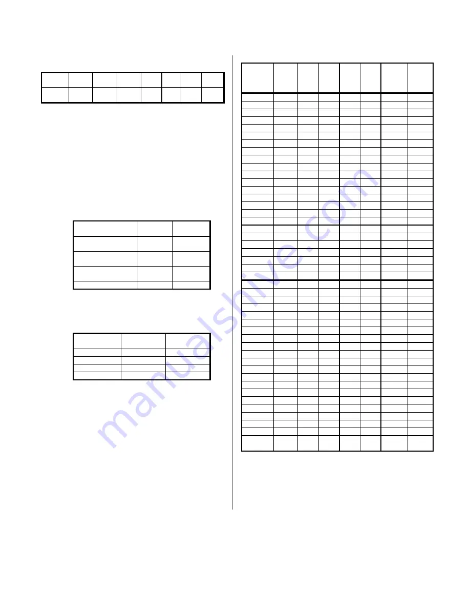
ODD Byte

MSB

D07

D06

D05

D04

D03

D02

D01

LSB

D00

GSEL

1

GSEL

0

Not

used

SEL

HIGH

CH3

CH2

CH1

CH0

RESET CONDITION: all bits are undefined.  Registers should be
programmed to the desired configuration before starting ADC analog
input acquisition.

Bit 15:          When read, the CTRIG bit indicates whether an ADC

conversion has been triggered, either by software
command or external trigger input.  If the bit reads high,
the conversion could be taking place or has been
completed.  CTRIG is cleared by reading the ADC data.
Writing to this bit position will have no effect.

Bits 14-10:   Not used - if read will return data written to those bit

positions.

Bits 9 & 8:   Control the input acquisition mode as described in the

following table:

Acquisition Mode

MODE1

Bit (D09)

MODE0

Bit (D08)

Differential Input

CH0-19 & CAL0-3

0

0

Single-ended Input

CH0-19

0

1

Single-ended Input

CH20-39

1

0

Auto Zero Input*

1

1

*  Auto Zero input is enabled by the mode bits,

overriding all channel selection bits.

Bits 7 & 6:   Control the programmable gain setting as described in

the following table:

Desired Gain

Setting

GSEL1

Bit (D07)

GSEL0

Bit (D06)

1

0

0

2

0

1

4

1

0

8

1

1

Bit 5:            Not used - if read will return data written to the bit

position.

Bit 4:           The SEL HIGH bit acts as the MSB for analog input

channel selection.  As such, its action is grouped with
that of bits 3-0 (see following).

Bits 3-0:      Control the selection of analog input channels per the

following table.  Note that the SEL HIGH bit and MODE
bits are also shown to completely define the channel
selection.  When MODE 1 & MODE 0 are both 0,
differential channels 0-19 and calibration voltages 0-3
may be selected; when MODE 1 is 0 and MODE 0 is 1,
single-ended channels 0-19 may be selected; when
MODE 1 is 1 and MODE 0 is 0, single-ended channels
20-39 may be selected; when both MODE 1 & MODE 0
are 1, the Auto Zero input is selected regardless of any
other bit levels.

Desired

Chan.

SEL

HIGH

Bit

D04

CH3

Bit

D03

CH2

Bit

D02

CH1

Bit

D01

CH0

Bit

D00

Mode

1

Bit

D09

Mode

0

Bit

D08

0

0

0

0

0

0

0

0/1

1

0

0

0

0

1

0

0/1

2

0

0

0

1

0

0

0/1

3

0

0

0

1

1

0

0/1

4

0

0

1

0

0

0

0/1

5

0

0

1

0

1

0

0/1

6

0

0

1

1

0

0

0/1

7

0

0

1

1

1

0

0/1

8

0

1

0

0

0

0

0/1

9

0

1

0

0

1

0

0/1

10

0

1

0

1

0

0

0/1

11

0

1

0

1

1

0

0/1

12

0

1

1

0

0

0

0/1

13

0

1

1

0

1

0

0/1

14

0

1

1

1

0

0

0/1

15

0

1

1

1

1

0

0/1

16

1

0

0

0

0

0

0/1

17

1

0

0

0

1

0

0/1

18

1

0

0

1

0

0

0/1

19

1

0

0

1

1

0

0/1

CAL0

1

0

1

0

0

0

0

CAL1

1

0

1

0

1

0

0

CAL2

1

0

1

1

0

0

0

CAL3

1

0

1

1

1

0

0

20

0

0

0

0

0

1

0

21

0

0

0

0

1

1

0

22

0

0

0

1

0

1

0

23

0

0

0

1

1

1

0

24

0

0

1

0

0

1

0

25

0

0

1

0

1

1

0

26

0

0

1

1

0

1

0

27

0

0

1

1

1

1

0

28

0

1

0

0

0

1

0

29

0

1

0

0

1

1

0

30

0

1

0

1

0

1

0

31

0

1

0

1

1

1

0

32

0

1

1

0

0

1

0

33

0

1

1

0

1

1

0

34

0

1

1

1

0

1

0

35

0

1

1

1

1

1

0

36

1

0

0

0

0

1

0

37

1

0

0

0

1

1

0

38

1

0

0

1

0

1

0

39

1

0

0

1

1

1

0

Auto
Zero

X

X

X

X

X

1

1

ADC Convert Command - (Write, Base + 10H)

The ADC Convert Command is a write only register (will not

respond to reads) that is used to trigger a conversion.  The data
written to this location should be all ones to reduce digital noise,
although the write action alone is sufficient to trigger the conversion.
Execution of this command requires 0 wait states.

Содержание IP320 Series

Страница 1: ...Board USER S MANUAL ACROMAG INCORPORATED 30765 South Wixom Road P O BOX 437 Wixom MI 48393 7037 U S A Tel 248 624 1541 Fax 248 624 9234 Copyright 1994 Acromag Inc Printed in the USA Data and specifications are subject to change without notice 8500 484 F00J005 retired ...

Страница 2: ... MECHANICAL ASSEMBLY 15 4501 435 ANALOG INPUT CONNECTION DIAGRAM 16 4501 436 BLOCK DIAGRAM 16 4501 462 CABLE 5025 550 NON SHIELDED 17 4501 463 CABLE 5025 551 SHIELDED 17 4501 464 TERMINATION PANEL 5025 552 18 4501 465 TRANSITION MODULE TRANS GP 18 IMPORTANT SAFETY CONSIDERATIONS It is very important for the user to consider the possible adverse effects of power wiring component sensor or software ...

Страница 3: ...able Model 5025 550 X or 5025 551 X INDUSTRIAL I O PACK SOFTWARE LIBRARY Acromag provides an Industrial I O Pack Software Library diskette Model IPSW LIB M03 MSDOS format to simplify communication with the board All functions are written in the C programming language and can be linked to your application Refer to the README TXT file in the root directory and the INFO320 TXT file in the IP320 subdi...

Страница 4: ...ol register is software configurable There are no hardware jumpers associated with it Control register bits are undefined at reset and must be programmed to the desired gain acquisition mode and channel configuration before starting ADC analog input acquisition refer to Section 3 for details Analog Input Data Format The analog input data will appear as Unipolar Straight Binary USB for unipolar inp...

Страница 5: ...ame location e g printed circuit board The channel density doubles when using single ended inputs and this a powerful incentive for their use However caution must be exercised since the single sense lead references all channels to the same common which will induce noise and offset if they are different The IP320 is non isolated since there is electrical continuity between the logic and field I O g...

Страница 6: ... not respond to addresses that are Not Used The function of each register noted in Table 3 1 will be discussed in the following sections IP Identification PROM Read Only 32 odd byte addresses Each IP module contains an identification ID PROM that resides in the ID space per the IP module specification This area of memory contains 32 bytes of information at most Both fixed and variable information ...

Страница 7: ... per the following table Note that the SEL HIGH bit and MODE bits are also shown to completely define the channel selection When MODE 1 MODE 0 are both 0 differential channels 0 19 and calibration voltages 0 3 may be selected when MODE 1 is 0 and MODE 0 is 1 single ended channels 0 19 may be selected when MODE 1 is 1 and MODE 0 is 0 single ended channels 20 39 may be selected when both MODE 1 MODE...

Страница 8: ...ates until it can deliver the data 7 Repeat steps 3 6 as required to acquire additional analog input samples Note that the input settling delay does not have to be inserted since writing to the control register to configure for the next acquisition immediately after initiating the previous conversion will allow the input to adequately settle before the next conversion is started The overlapping of...

Страница 9: ...ur voltages and the analog ground reference are used to determine the endpoints of a straight line which defines the analog input characteristic The calibration voltages are precisely adjusted at the factory to provide optimum performance as detailed in the following table Calibration Signal Ideal Value Volts Maximum Tolerance 25oC Volts Maximum Temperature Drift ppm oC Auto Zero 0 0000 0 0002 0 C...

Страница 10: ...ts are set to zero 2 Delay to allow for input settling 3 Execute ADC Convert Command Base 10H 4 Execute Read ADC Data Command Base 20H Note that the 12 bit data is left justified within the 16 bit word 5 Repeat steps 3 and 4 several times e g 16 and take the average of the ADC results Save this number as CountCALLO 6 To prepare to measure CountCALHI write to the Control Register Base 00H to setup ...

Страница 11: ...y possible for each range It is the sum of error components due to ADC quantization of the low and high calibration signals PGA and ADC linearity error and the absolute errors of the recommended calibration voltages at 25oC Typical accuracies are significantly better Table 3 6 Maximum Overall Calibrated Error 25 C Input Range Volts PGA Gain ADC Range Volts Max Error LSB Span 5 to 5 1 5 to 5 1 8 0 ...

Страница 12: ...nput circuitry The ID PROM control register and ADC data are all accessed through the 16 bit data bus interface to the carrier board 5 0 SERVICE AND REPAIR SERVICE AND REPAIR ASSISTANCE Surface Mounted Technology SMT boards are generally difficult to repair It is highly recommended that a non functioning board be returned to Acromag for repair The board can be damaged unless special SMT repair and...

Страница 13: ...e programmable gain to determine the actual input range Input signal ranges may actually fall short of reaching the specified endpoints due to hardware limitations For example if an input may reach zero volts or less a bipolar input range should be selected 3 These ranges can only be achieved with 15 Volt external power supplies The input ranges will be clipped if 12 Volt supplies are used typical...

Страница 14: ...n assignments Refer to the IP module manual for correct wiring connections to the termination panel Schematic and Physical Attributes See Drawing 4501 464 Field Wiring 50 position terminal blocks with screw clamps Wire range 12 to 26 AWG Connections to AVME9630 9660 P1 50 pin male header with strain relief ejectors Use Acromag 5025 550 x or 5025 551 x cable to connect panel to VME board Keep cable...

Страница 15: ...SERIES IP320 INDUSTRIAL I O PACK 12 BIT HIGH DENSITY ANALOG INPUT BOARD ___________________________________________________________________________________________ 15 ...

Страница 16: ...SERIES IP320 INDUSTRIAL I O PACK 12 BIT HIGH DENSITY ANALOG INPUT BOARD ___________________________________________________________________________________________ 16 ...

Страница 17: ...SERIES IP320 INDUSTRIAL I O PACK 12 BIT HIGH DENSITY ANALOG INPUT BOARD ___________________________________________________________________________________________ 17 ...

Страница 18: ...SERIES IP320 INDUSTRIAL I O PACK 12 BIT HIGH DENSITY ANALOG INPUT BOARD ___________________________________________________________________________________________ 18 ...

Отзывы: