System Introduction
1-
29
1.4.26
AC Adapter
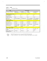
Table 1-34
AC Adapter Specifications
Item
Specification
Vendor & model name
Delta ADP-45GB REV.E2
Input Requirements
Nominal voltages (Vrms)
90 - 264
Frequency variation range (Hz)
47 - 63
Maximum input current (A, @90Vac, full load)
1.5 A
Inrush current
The maximum inrush current will be less than 50A and 100A
when the adapter is connected to 115Vac(60Hz) and
230Vac(50Hz) respectively.
Efficiency
It should provide an efficiency of 83% minimum, when
measured at maximum load under 115V(60Hz)
Output Ratings (CV mode)
DC output voltage (V)
+19
Noise + Ripple (mV)
300
Load (A)
0 (min.)
2.4 (max.)
Dynamic Output Characteristics
Turn-on delay time (s, @115Vac)
2
Hold up time (ms; @115 Vac input, full load)
5 (min.)
Over Voltage Protection (OVP, V)
26
Short circuit protection
Output can be shorted without damage
Electrostatic discharge (ESD, kV)
±
15 (at air discharge)
Dielectric Withstand Voltage
Primary to secondary
3000 Vac (or 4242 Vdc), 10 mA for 1 second
Leakage current
0.25 mA maximum @ 254 Vac, 60Hz.
Regulatory Requirements
Internal filter meets:
1.
FCC class B requirements.
2.
CISPR 22 Class B requirements.
Содержание Extensa 61X
Страница 1: ...TI Extensa 61X Series AcerNote 370P Notebook Service Guide PART NO 2238309 0809 DOC NO PRINTED IN USA ...
Страница 6: ...vi ...
Страница 26: ...1 8 Service Guide Figure 1 5 Main Board Layout Bottom Side ...
Страница 49: ...System Introduction 1 31 1 5 1 3 Power Management Figure 1 14 Power Management Block Diagram ...
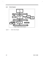
Страница 55: ...System Introduction 1 37 1 6 System Block Diagram Figure 1 15 System Block Diagram ...
Страница 64: ...Major Chips Description 2 7 2 2 5 Pin Diagram Figure 2 4 M1521 Pin Diagram ...
Страница 99: ...2 42 Service Guide 2 5 3 Pin Diagram Figure 2 10 C T 65550 Pin Diagram ...
Страница 116: ...Major Chips Description 2 59 2 6 4 Block Diagram Figure 2 11 Functional Block Diagram 16 bit PC Card Interface ...
Страница 117: ...2 60 Service Guide Figure 2 12 Functional block diagram CardBus Card Interface ...
Страница 118: ...Major Chips Description 2 61 2 6 5 Pin Diagram Figure 2 13 PCI to PC Card 16 bit terminal assignments ...
Страница 119: ...2 62 Service Guide Figure 2 14 PCI to CardBus terminal assignments ...
Страница 135: ...2 78 Service Guide 2 7 3 Pin Diagram Figure 2 16 NS87336VJG Pin Diagram ...
Страница 145: ...2 88 Service Guide 2 8 2 Pin Diagram Figure 2 17 YMF715 Block Diagram ...
Страница 185: ...Disassembly and Unit Replacement 4 5 Figure 4 3 Disassembly Sequence Flowchart ...
Страница 209: ...B 2 Service Guide ...
Страница 210: ...Exploded View Diagram B 3 ...
Страница 217: ...A p p e n d i x D A p p e n d i x D Schematics This appendix shows the schematic diagrams of the notebook ...

